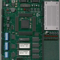
MPC555CME Freescale Semiconductor, MPC555CME Datasheet - Page 648

MPC555CME
Manufacturer Part Number
MPC555CME
Description
KIT EVALUATION FOR MPC555
Manufacturer
Freescale Semiconductor
Type
Microcontrollerr
Datasheet
1.MPC555CME.pdf
(966 pages)
Specifications of MPC555CME
Contents
Module Board, Installation Guide, Power Supply, Cable, Software and more
Processor To Be Evaluated
MPC555
Data Bus Width
32 bit
Interface Type
RS-232
For Use With/related Products
MPC555
Lead Free Status / RoHS Status
Contains lead / RoHS non-compliant
- Current page: 648 of 966
- Download datasheet (13Mb)
MISRH — Multiple Input Signature Register High
MISRL — Multiple Input Signature Register Low
MISCNT — MISC Counter
RESET:
RESET:
RESET:
18.3.5 MISC Counter (MISCNT)
18.4 Operation
18.4.1 Normal Operation
18.4.2 Standby Operation
MPC555
USER’S MANUAL
MSB
MSB
D31
D15
0
0
0
0
The MISCNT contains the address of the current MISC memory access. This registers
is read-only. Note that the naming of the A[31:0] bits represents little-endian bit encod-
ing.
Exiting TPU3 emulation mode or clearing the MISEN bit in the DPTMCR results in the
reset of this register.
The DPTRAM module has several modes of operation. The following sections de-
scribe DPTRAM operation in each of these modes.
In normal operation, the DPTRAM is powered by V
IMB3 by a bus master.
Read or write accesses of 8, 16, or 32 bits are supported. In normal operation, neither
TPU3 accesses the array, nor do they have any effect on the operation of the DP-
TRAM module.
The DPTRAM array uses a separate power supply VDDSRAM to maintain the con-
tents of the DPTRAM array during a power-down phase.
When the RAM array is powered by the VDDSRAM pin of the MCU, access to the RAM
array is blocked. Data read from the RAM array during this condition cannot be guar-
anteed. Data written to the DPTRAM may be corrupted if switching occurs during a
write operation.
RESERVED
D30
D14
1
0
1
0
/
MPC556
D29
D13
2
0
2
0
A12
D28
D12
3
0
3
0
A11
D27
D11
4
0
4
0
A10
D26
D10
DUAL-PORT TPU RAM (DPTRAM)
5
0
5
0
Rev. 15 October 2000
D25
A9
D9
6
0
6
0
Last Memory Address
D24
A8
D8
7
0
7
0
D23
A7
D7
8
0
8
0
D22
A6
D6
9
0
9
0
DDL
D21
A5
10
D5
10
0
0
and may be accessed via the
D20
11
A4
D4
11
0
0
D19
A3
12
D3
12
0
0
D18
13
A2
D2
13
0
0
0x30 0006
0x30 0008
0x30 000A
MOTOROLA
D17
A1
14
D1
14
0
0
LSB
18-6
LSB
D16
15
A0
D0
15
0
0
Related parts for MPC555CME
Image
Part Number
Description
Manufacturer
Datasheet
Request
R

Part Number:
Description:
MPC555 Interrupts
Manufacturer:
Freescale Semiconductor / Motorola
Datasheet:
Part Number:
Description:
Manufacturer:
Freescale Semiconductor, Inc
Datasheet:
Part Number:
Description:
Manufacturer:
Freescale Semiconductor, Inc
Datasheet:
Part Number:
Description:
Manufacturer:
Freescale Semiconductor, Inc
Datasheet:
Part Number:
Description:
Manufacturer:
Freescale Semiconductor, Inc
Datasheet:
Part Number:
Description:
Manufacturer:
Freescale Semiconductor, Inc
Datasheet:
Part Number:
Description:
Manufacturer:
Freescale Semiconductor, Inc
Datasheet:
Part Number:
Description:
Manufacturer:
Freescale Semiconductor, Inc
Datasheet:
Part Number:
Description:
Manufacturer:
Freescale Semiconductor, Inc
Datasheet:
Part Number:
Description:
Manufacturer:
Freescale Semiconductor, Inc
Datasheet:
Part Number:
Description:
Manufacturer:
Freescale Semiconductor, Inc
Datasheet:
Part Number:
Description:
Manufacturer:
Freescale Semiconductor, Inc
Datasheet:
Part Number:
Description:
Manufacturer:
Freescale Semiconductor, Inc
Datasheet:
Part Number:
Description:
Manufacturer:
Freescale Semiconductor, Inc
Datasheet:
Part Number:
Description:
Manufacturer:
Freescale Semiconductor, Inc
Datasheet:


