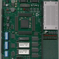
MPC555CME Freescale Semiconductor, MPC555CME Datasheet - Page 372

MPC555CME
Manufacturer Part Number
MPC555CME
Description
KIT EVALUATION FOR MPC555
Manufacturer
Freescale Semiconductor
Type
Microcontrollerr
Datasheet
1.MPC555CME.pdf
(966 pages)
Specifications of MPC555CME
Contents
Module Board, Installation Guide, Power Supply, Cable, Software and more
Processor To Be Evaluated
MPC555
Data Bus Width
32 bit
Interface Type
RS-232
For Use With/related Products
MPC555
Lead Free Status / RoHS Status
Contains lead / RoHS non-compliant
- Current page: 372 of 966
- Download datasheet (13Mb)
10.4 Global (Boot) Chip-Select Operation
MPC555
USER’S MANUAL
Global (boot) chip-select operation allows address decoding for a boot ROM before
system initialization. CS[0] is the global chip-select output. Its operation differs from
that of the other external chip-select outputs following a system reset. When the RCPU
begins accessing memory after a system reset, CS[0] is asserted for every address,
unless an internal device (register) is accessed.
The global chip select provides a programmable port size at system reset using the
reset BPS pins ([4:5]) of the reset configuration word, allowing a boot ROM to be lo-
cated anywhere in the address space. For more information, see
Configuration
sponds to all address types. CS[0] operates in this way until the first write to the CS[0]
option register (OR0). The pin can be programmed to continue decoding a range of
addresses after this write, provided the preferred address range is first loaded into
base register zero. After the first write to OR0, the global chip select can only be re-
started with a system reset.
The memory controller operates in boot mode until the user modifies the values in OR0
and BR to the ones desired.
Table 10-3
/
MPC556
If the MPC555 / MPC556 is configured (in the reset configuration
word) to use the internal flash EEPROM as boot memory CS[0] is not
asserted.
shows the initial values of the “boot bank” in the memory controller.
Table 10-3 Boot Bank Fields Values After Hard Reset
Word. The global chip select does not provide write protection and re-
BSCY[0:2]
ATM
AM[0:16]
ACS[0:1]
SCY[0:3]
CSNT
SETA
TRLX
Field
WP
PS
BI
V
[
0:2]
MEMORY CONTROLLER
Rev. 15 October 2000
From reset configuration
From reset configuration
0 0000 0000 0000 0000
NOTE
Value (Binary)
1111
000
011
00
0
0
1
0
0
7.5.2 Hard Reset
MOTOROLA
10-20
Related parts for MPC555CME
Image
Part Number
Description
Manufacturer
Datasheet
Request
R

Part Number:
Description:
MPC555 Interrupts
Manufacturer:
Freescale Semiconductor / Motorola
Datasheet:
Part Number:
Description:
Manufacturer:
Freescale Semiconductor, Inc
Datasheet:
Part Number:
Description:
Manufacturer:
Freescale Semiconductor, Inc
Datasheet:
Part Number:
Description:
Manufacturer:
Freescale Semiconductor, Inc
Datasheet:
Part Number:
Description:
Manufacturer:
Freescale Semiconductor, Inc
Datasheet:
Part Number:
Description:
Manufacturer:
Freescale Semiconductor, Inc
Datasheet:
Part Number:
Description:
Manufacturer:
Freescale Semiconductor, Inc
Datasheet:
Part Number:
Description:
Manufacturer:
Freescale Semiconductor, Inc
Datasheet:
Part Number:
Description:
Manufacturer:
Freescale Semiconductor, Inc
Datasheet:
Part Number:
Description:
Manufacturer:
Freescale Semiconductor, Inc
Datasheet:
Part Number:
Description:
Manufacturer:
Freescale Semiconductor, Inc
Datasheet:
Part Number:
Description:
Manufacturer:
Freescale Semiconductor, Inc
Datasheet:
Part Number:
Description:
Manufacturer:
Freescale Semiconductor, Inc
Datasheet:
Part Number:
Description:
Manufacturer:
Freescale Semiconductor, Inc
Datasheet:
Part Number:
Description:
Manufacturer:
Freescale Semiconductor, Inc
Datasheet:


