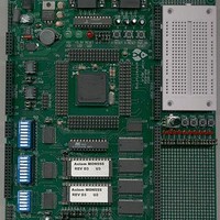
MPC555CME Freescale Semiconductor, MPC555CME Datasheet - Page 649

MPC555CME
Manufacturer Part Number
MPC555CME
Description
KIT EVALUATION FOR MPC555
Manufacturer
Freescale Semiconductor
Type
Microcontrollerr
Datasheet
1.MPC555CME.pdf
(966 pages)
Specifications of MPC555CME
Contents
Module Board, Installation Guide, Power Supply, Cable, Software and more
Processor To Be Evaluated
MPC555
Data Bus Width
32 bit
Interface Type
RS-232
For Use With/related Products
MPC555
Lead Free Status / RoHS Status
Contains lead / RoHS non-compliant
- Current page: 649 of 966
- Download datasheet (13Mb)
18.4.3 Reset Operation
18.4.4 Stop Operation
MPC555
USER’S MANUAL
In order to guarantee valid DPTRAM data during power-down, external low voltage in-
hibit circuitry (external to the MCU) must be designed to force the RESET pin of the
MCU into the active state before VDDL drops below its normal limit. This is necessary
to inhibit spurious writes to the DPTRAM during power-down.
When a synchronous reset occurs, a bus master is allowed to complete the current
access. Thus a write bus cycle (byte or half word) that is in progress when a synchro-
nous reset occurs will be completed without error. Once a write already in progress
has been completed, further writes to the RAM array are inhibited.
If a reset is generated by an asynchronous reset such as the loss of clocks or software
watchdog time-out, the contents of the RAM array are not guaranteed. (Refer to
TION 7 RESET
trol, and status.)
Reset will also reconfigure some of the fields and bits in the DPTRAM control registers
to their default reset state. See the description of the control registers to determine the
effect of reset on these registers.
Setting the STOP control bit in the DPTMCR causes the module to enter its lowest
power-consuming state. The DPTMCR can still be written to allow the STOP control
bit to be cleared.
In stop mode, the DPTRAM array cannot be read or written. All data in the array is re-
tained. The BIU continues to operate to allow the CPU to access the STOP bit in the
DPTMCR. The system clock remains stopped until the STOP bit is cleared or the DP-
TRAM module is reset.
The STOP bit is initialized to logical zero during reset. Only the STOP bit in the DPT-
MCR can be accessed while the STOP bit is asserted. Accesses to other DPTRAM
registers may result in unpredictable behavior. Note also that the STOP bit should be
set and cleared independently of the other control bits in this register to guarantee
proper operation. Changing the state of other bits while changing the state of the
STOP bit may result in unpredictable behavior.
/
MPC556
A word (32-bit) write will be completed coherently only if the reset oc-
curs during the second (16-bit) write bus cycle. If reset occurs during
the first write bus cycle, only the first half word will be written to the
RAM array and the second write will not be allowed to occur. In this
case, the word data contained in the DPTRAM will not be coherent.
The first half word will contain the most significant half of the new
word information and the second half word will contain the least sig-
nificant half of the old word information.
for a description of MPC555 / MPC556 reset sources, operation, con-
DUAL-PORT TPU RAM (DPTRAM)
Rev. 15 October 2000
NOTE
MOTOROLA
SEC-
18-7
Related parts for MPC555CME
Image
Part Number
Description
Manufacturer
Datasheet
Request
R

Part Number:
Description:
MPC555 Interrupts
Manufacturer:
Freescale Semiconductor / Motorola
Datasheet:
Part Number:
Description:
Manufacturer:
Freescale Semiconductor, Inc
Datasheet:
Part Number:
Description:
Manufacturer:
Freescale Semiconductor, Inc
Datasheet:
Part Number:
Description:
Manufacturer:
Freescale Semiconductor, Inc
Datasheet:
Part Number:
Description:
Manufacturer:
Freescale Semiconductor, Inc
Datasheet:
Part Number:
Description:
Manufacturer:
Freescale Semiconductor, Inc
Datasheet:
Part Number:
Description:
Manufacturer:
Freescale Semiconductor, Inc
Datasheet:
Part Number:
Description:
Manufacturer:
Freescale Semiconductor, Inc
Datasheet:
Part Number:
Description:
Manufacturer:
Freescale Semiconductor, Inc
Datasheet:
Part Number:
Description:
Manufacturer:
Freescale Semiconductor, Inc
Datasheet:
Part Number:
Description:
Manufacturer:
Freescale Semiconductor, Inc
Datasheet:
Part Number:
Description:
Manufacturer:
Freescale Semiconductor, Inc
Datasheet:
Part Number:
Description:
Manufacturer:
Freescale Semiconductor, Inc
Datasheet:
Part Number:
Description:
Manufacturer:
Freescale Semiconductor, Inc
Datasheet:
Part Number:
Description:
Manufacturer:
Freescale Semiconductor, Inc
Datasheet:


