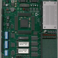
MPC555CME Freescale Semiconductor, MPC555CME Datasheet - Page 258

MPC555CME
Manufacturer Part Number
MPC555CME
Description
KIT EVALUATION FOR MPC555
Manufacturer
Freescale Semiconductor
Type
Microcontrollerr
Datasheet
1.MPC555CME.pdf
(966 pages)
Specifications of MPC555CME
Contents
Module Board, Installation Guide, Power Supply, Cable, Software and more
Processor To Be Evaluated
MPC555
Data Bus Width
32 bit
Interface Type
RS-232
For Use With/related Products
MPC555
Lead Free Status / RoHS Status
Contains lead / RoHS non-compliant
- Current page: 258 of 966
- Download datasheet (13Mb)
7.5.2 Hard Reset Configuration Word
MPC555
USER’S MANUAL
Hard Reset Configuration Word
PRPM
EARB
MSB
Bit(s)
9:10
DEFAULT:
16
DEFAULT:
4:5
6:8
0
0
0
0
1
2
3
The hard reset configuration word, which is sampled from the internal data bus on the
negation of HRESET, is shown below. The reset configuration word is not a register in
the memory map. Most of the bits in the configuration are located in registers in the
USIU. The user should refer to the appropriate register definition for a detailed descrip-
tion of each control bit.
17
IP
/
1
0
0
MPC556
SC
DBGC
Name
EARB
BDRV
BDIS
BPS
BDRV
IP
—
Table 7-5 Hard Reset Configuration Word Bit Descriptions
18
2
0
0
ETRE FLEN
BDIS
19
External arbitration. Refer to
definition.
0 = Internal arbitration is performed
1 = External arbitration is assumed
Initial interrupt prefix. This bit defines the initial value of the MSR[IP] bit immediately after re-
set. MSR[IP] defines the interrupt table location.
0 = MSR[IP] = 0 after reset
1 = MSR[IP] = 1 after reset
Bus pins drive strength. This bit determines the driving capability of the bus pins (address,
data, and control) and the CLKOUT pin. For details, refer to description of the COM bits in
8.12.1 System Clock Control Register
the bus pins and CLKOUT.
0 = Full drive
1 = Reduced drive
External boot disable. If a write to the OR0 register occurs after reset, this bit definition is ig-
0 = Memory controller bank 0 is active and matches all addresses immediately after reset
1 = Memory controller is not activated after reset.
Boot port size. If a write to the OR0 register occurs after reset, this field definition is ignored.
00 = 32-bit port (default)
01 = 8-bit port
10 = 16-bit port
11 = Reserved
Reserved
Debug pins configuration. See
definition. The default value is for these pins to function as VFLS[0:1], BI, BR, BG, and BB.
3
0
0
nored.
20
4
0
0
BPS
COMP
EN_
21
5
0
0
COMP
EXC_
Rev. 15 October 2000
22
6
0
0
Reserved
SERVED
RE-
6.13.1.1 SIU Module Configuration Register
23
7
0
0
RESET
6.13.1.1 SIU Module Configuration Register
24
8
0
0
Description
(SCCR). The default value is full drive strength for
25
9
0
Reserved
0
DBGC
10
26
0
0
DBPC ATWC
11
27
0
0
12
28
0
0
ISB
13
29
0
0
EBDF
for a detailed bit
for this field
MOTOROLA
14
30
0
0
served
DME
LSB
Re-
15
31
7-12
0
0
Related parts for MPC555CME
Image
Part Number
Description
Manufacturer
Datasheet
Request
R

Part Number:
Description:
MPC555 Interrupts
Manufacturer:
Freescale Semiconductor / Motorola
Datasheet:
Part Number:
Description:
Manufacturer:
Freescale Semiconductor, Inc
Datasheet:
Part Number:
Description:
Manufacturer:
Freescale Semiconductor, Inc
Datasheet:
Part Number:
Description:
Manufacturer:
Freescale Semiconductor, Inc
Datasheet:
Part Number:
Description:
Manufacturer:
Freescale Semiconductor, Inc
Datasheet:
Part Number:
Description:
Manufacturer:
Freescale Semiconductor, Inc
Datasheet:
Part Number:
Description:
Manufacturer:
Freescale Semiconductor, Inc
Datasheet:
Part Number:
Description:
Manufacturer:
Freescale Semiconductor, Inc
Datasheet:
Part Number:
Description:
Manufacturer:
Freescale Semiconductor, Inc
Datasheet:
Part Number:
Description:
Manufacturer:
Freescale Semiconductor, Inc
Datasheet:
Part Number:
Description:
Manufacturer:
Freescale Semiconductor, Inc
Datasheet:
Part Number:
Description:
Manufacturer:
Freescale Semiconductor, Inc
Datasheet:
Part Number:
Description:
Manufacturer:
Freescale Semiconductor, Inc
Datasheet:
Part Number:
Description:
Manufacturer:
Freescale Semiconductor, Inc
Datasheet:
Part Number:
Description:
Manufacturer:
Freescale Semiconductor, Inc
Datasheet:


