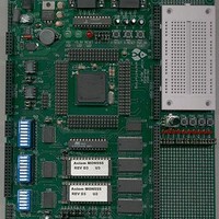
MPC555CME Freescale Semiconductor, MPC555CME Datasheet - Page 686

MPC555CME
Manufacturer Part Number
MPC555CME
Description
KIT EVALUATION FOR MPC555
Manufacturer
Freescale Semiconductor
Type
Microcontrollerr
Datasheet
1.MPC555CME.pdf
(966 pages)
Specifications of MPC555CME
Contents
Module Board, Installation Guide, Power Supply, Cable, Software and more
Processor To Be Evaluated
MPC555
Data Bus Width
32 bit
Interface Type
RS-232
For Use With/related Products
MPC555
Lead Free Status / RoHS Status
Contains lead / RoHS non-compliant
- Current page: 686 of 966
- Download datasheet (13Mb)
MPC555
USER’S MANUAL
the value of the NVM fuse. Reading CENSOR[0:1] while setting or clearing with the
high voltage applied (CSC = 1 and EHV = 1) will return zeroes.
The set operation changes the state in an NVM fuse from a zero to a one by program-
ming NVM bit 0 and erasing NVM bit 1 simultaneously in the NVM fuse. This set oper-
ation can be performed without changing the contents of the CMF array.
To set one or both of the bits in CENSOR[0:1],
The clear operation changes the state in an NVM fuse from a one to a zero by erasing
NVM bit 0 and programming NVM bit 1 simultaneously in the NVM fuse. This clear op-
eration can be done only while erasing the entire CMF array and shadow information.
To clear CENSOR[0:1],
1. Using section
2. Write a one to the CENSOR bit(s) to be set.
3. Write EHV = 1 in the CMFCTL register. This will apply the programming voltag-
4. Read the CMFCTL register until HVS = 0.
5. Write EHV = 0 in the CMFCTL register.
6. Read the CMFMCR CENSOR bit(s) that are being set. If any bit selected for set
7. Write SES = 0 and CSC = 0.
1. Write PROTECT[0:7] = 0x00 to enable the entire array for erasure.
2. Using section
3. Perform an erase interlock write.
4. Write EHV = 1 in the CMFCTL register. This will apply the erase voltages to the
5. Read the CMFCTL register until HVS = 0.
6. Write EHV = 0 in the CMFCTL register.
7. Read the entire CMF array and the shadow information words. If any bit equals
8. Read CENSOR[0:1]. If CENSOR[0:1]
9. Write SES = 0 and CSC = 0.
/
Programmed
Programmed
MPC556
NVM bit 0
CLKPM, write the pulse width timing control fields for an erase pulse, CSC = 1,
PE = 0 and SES = 1 in the CMFCTL register.
es to NVM bit 0 and the erase voltages to NVM bit 1 simultaneously.
is a 0 go to step 3.
CLKPM, write the pulse width timing control fields for an erase pulse,
BLOCK[0:7] = 0xFF, CSC = 1, PE = 1 and SES = 1 in the CMFCTL register.
entire CMF array and NVM bit 0 and the programming voltages to NVM bit 1
simultaneously.
zero, go to step 4.
Erased
Erased
19.7.6 A Technique to Determine SCLKR, CLKPE, and
19.7.6 A Technique to Determine SCLKR, CLKPE, and
Table 19-17 NVM Fuse States
CDR MoneT FLASH EEPROM
Rev. 15 October 2000
Programmed
Programmed
NVM bit 1
Erased
Erased
≠
0 go to step 4.
NVM Fuse Bit Value
Cleared (0)
Undefined
Undefined
Set (1)
MOTOROLA
19-34
Related parts for MPC555CME
Image
Part Number
Description
Manufacturer
Datasheet
Request
R

Part Number:
Description:
MPC555 Interrupts
Manufacturer:
Freescale Semiconductor / Motorola
Datasheet:
Part Number:
Description:
Manufacturer:
Freescale Semiconductor, Inc
Datasheet:
Part Number:
Description:
Manufacturer:
Freescale Semiconductor, Inc
Datasheet:
Part Number:
Description:
Manufacturer:
Freescale Semiconductor, Inc
Datasheet:
Part Number:
Description:
Manufacturer:
Freescale Semiconductor, Inc
Datasheet:
Part Number:
Description:
Manufacturer:
Freescale Semiconductor, Inc
Datasheet:
Part Number:
Description:
Manufacturer:
Freescale Semiconductor, Inc
Datasheet:
Part Number:
Description:
Manufacturer:
Freescale Semiconductor, Inc
Datasheet:
Part Number:
Description:
Manufacturer:
Freescale Semiconductor, Inc
Datasheet:
Part Number:
Description:
Manufacturer:
Freescale Semiconductor, Inc
Datasheet:
Part Number:
Description:
Manufacturer:
Freescale Semiconductor, Inc
Datasheet:
Part Number:
Description:
Manufacturer:
Freescale Semiconductor, Inc
Datasheet:
Part Number:
Description:
Manufacturer:
Freescale Semiconductor, Inc
Datasheet:
Part Number:
Description:
Manufacturer:
Freescale Semiconductor, Inc
Datasheet:
Part Number:
Description:
Manufacturer:
Freescale Semiconductor, Inc
Datasheet:


