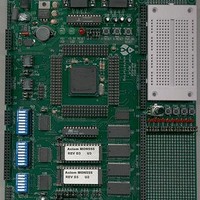
MPC555CME Freescale Semiconductor, MPC555CME Datasheet - Page 678

MPC555CME
Manufacturer Part Number
MPC555CME
Description
KIT EVALUATION FOR MPC555
Manufacturer
Freescale Semiconductor
Type
Microcontrollerr
Datasheet
1.MPC555CME.pdf
(966 pages)
Specifications of MPC555CME
Contents
Module Board, Installation Guide, Power Supply, Cable, Software and more
Processor To Be Evaluated
MPC555
Data Bus Width
32 bit
Interface Type
RS-232
For Use With/related Products
MPC555
Lead Free Status / RoHS Status
Contains lead / RoHS non-compliant
- Current page: 678 of 966
- Download datasheet (13Mb)
19.6.2 Erase Margin Reads
19.6.3 Erasing Shadow Information Words
MPC555
USER’S MANUAL
State
S1
S2
S3
S4
S5
The CMF EEPROM provides an erase margin read with electrical margin for the erase
state. Erase margin reads provide sufficient margin to ensure specified data retention.
The erase margin read is enabled when SES = 1 and the erase write has occurred.
The erase margin read and subsequent on-page erase verify reads return a zero for
any bit that has not been completely erased. Bits that have completed erasing return
one when read. To increase the access time of the erase margin read, the off-page
access time is 16 clocks instead of the usual two clock off-page read access time. The
erase margin read occurs during an off-page read. All locations within the block(s) be-
ing erased must return one when read to determine that no more erase pulses are re-
quired.
The shadow information words are erased with CMF array block zero. To verify that
the shadow information words are erased, the SIE bit in CMFMCR must be set to one
Normal Operation:
Normal array reads and register accesses. The
Block protect information and pulse width timing
control can be modified.
Erase Hardware Interlock Write:
Normal read operation still occurs. The CMF ac-
cepts the erase hardware interlock write. This write
may be to any CMF array location. Accesses to the
registers are normal register accesses. A write to
CMFCTL can not set EHV at this time. A write to
the register is not an erase hardware interlock
write, and the CMF remains in state S2.
High Voltage Write Enable
Erase margin reads will occur. Accesses to the
registers are normal register accesses. A write to
CMFCTL can change EHV.
Erase Operation:
High voltage is applied to the array blocks to erase
the CMF bit cells. The pulse width timer is active if
SCLKR[0:2] ≠ 0, and HVS can be polled to time the
erase pulse. During the erase operation, the array
does not respond to any address. Accesses to the
registers are allowed. A write to CMFCTL can
change EHV only.
Erase Margin Read Operation:
These reads determine whether the state of the
bits in the selected blocks needs further modifica-
tion by the erase operation. Once a bit is fully
erased it returns one when read. All words within
the blocks being erased must be read to determine
whether the erase operation is completed.
/
MPC556
Table 19-11 Erase Interlock State Descriptions
Mode
CDR MoneT FLASH EEPROM
Rev. 15 October 2000
State
Next
S2
S1
S3
S1
S4
S1
S5
S4
S1
T2
T1
T3
T6
T4
T7
T5
T8
T9
A successful write to any CMF array lo-
cation is the erase interlock write. If the
ware interlock write has not been done
and the CMF will remain in state S2.
write is to a register the erase hard-
Write EHV = 0, disable the internal
Write SES = 0 or a master reset
Write SES = 0 or a master reset
Write SES = 0 or a master reset
Transition Requirement
memory map or a soft reset
Write PE = 1, SES = 1.
Hardware Interlock
Write EHV = 1
Write EHV=1
Master reset
MOTOROLA
19-26
Related parts for MPC555CME
Image
Part Number
Description
Manufacturer
Datasheet
Request
R

Part Number:
Description:
MPC555 Interrupts
Manufacturer:
Freescale Semiconductor / Motorola
Datasheet:
Part Number:
Description:
Manufacturer:
Freescale Semiconductor, Inc
Datasheet:
Part Number:
Description:
Manufacturer:
Freescale Semiconductor, Inc
Datasheet:
Part Number:
Description:
Manufacturer:
Freescale Semiconductor, Inc
Datasheet:
Part Number:
Description:
Manufacturer:
Freescale Semiconductor, Inc
Datasheet:
Part Number:
Description:
Manufacturer:
Freescale Semiconductor, Inc
Datasheet:
Part Number:
Description:
Manufacturer:
Freescale Semiconductor, Inc
Datasheet:
Part Number:
Description:
Manufacturer:
Freescale Semiconductor, Inc
Datasheet:
Part Number:
Description:
Manufacturer:
Freescale Semiconductor, Inc
Datasheet:
Part Number:
Description:
Manufacturer:
Freescale Semiconductor, Inc
Datasheet:
Part Number:
Description:
Manufacturer:
Freescale Semiconductor, Inc
Datasheet:
Part Number:
Description:
Manufacturer:
Freescale Semiconductor, Inc
Datasheet:
Part Number:
Description:
Manufacturer:
Freescale Semiconductor, Inc
Datasheet:
Part Number:
Description:
Manufacturer:
Freescale Semiconductor, Inc
Datasheet:
Part Number:
Description:
Manufacturer:
Freescale Semiconductor, Inc
Datasheet:


