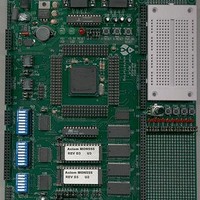
MPC555CME Freescale Semiconductor, MPC555CME Datasheet - Page 662

MPC555CME
Manufacturer Part Number
MPC555CME
Description
KIT EVALUATION FOR MPC555
Manufacturer
Freescale Semiconductor
Type
Microcontrollerr
Datasheet
1.MPC555CME.pdf
(966 pages)
Specifications of MPC555CME
Contents
Module Board, Installation Guide, Power Supply, Cable, Software and more
Processor To Be Evaluated
MPC555
Data Bus Width
32 bit
Interface Type
RS-232
For Use With/related Products
MPC555
Lead Free Status / RoHS Status
Contains lead / RoHS non-compliant
- Current page: 662 of 966
- Download datasheet (13Mb)
MPC555
USER’S MANUAL
Bit(s)
16:23
9:15
2:4
6:7
24
25
0
1
5
8
/
CLKPM
SCLKR
BLOCK
CLKPE
MPC556
Name
HVS
CSC
[0:7]
—
—
—
—
High voltage status. During a program or erase pulse this bit is set while the pulse is active or
during recovery. The BIU does not acknowledge an access to an array location if HVS = 1. While
HVS = 1, SES cannot be changed. This bit is read only; writes have no effect.
0 = Program or erase pulse is not applied to the CMF array or shadow information
1 = Program or erase pulse is applied to the CMF array or shadow information
Reserved
System clock range. These bits are write protected by the SES bit. Writes to CMFCTL do not
change SCLKR[0:2] if SES = 1. The default reset state of SCLKR[0:2] = 000 for a clock scaling
of 1.
000 = Clock scaling of 1 (Not for Customer use.)
001 = Clock scaling of 1
010 = Clock scaling of 3/2
011 = Clock scaling of 2
100 = Clock scaling of 3
101 = Clock scaling of 4
110 = Reserved
111 = Reserved
Refer to
Reserved
Clock period exponent. The CLKPE, CSC, and PE fields determine the value of the exponential
clock multiplier, N. Refer to
The CLKPE bits are write protected by the SES bit. Writes to CMFCTL will not change CLKPE
if SES = 1.The default reset state of CLKPE is 00.
Reserved
Clock period multiple. This field determines the linear clock multiplier, M, according to the follow-
ing equation:
M = 1 + CLKPM[0:6]
The CLKPM bits are write protected by the SES bit. Writes to CMFCTL will not change CLKPM
if SES = 1. The reset state of CLKPM = 0, for a multiplier of 1. Refer to
Multiplier
Block program and erase select. The CMF EEPROM array blocks that are selected to be pro-
grammed or erased are the blocks for which BLOCK[M] = 1.
Bit 16 controls block 0 and bit 23 controls block 7. On the 192-Kbyte array (Flash Module B),
blocks 6 and 7 are not available, but these bits need to be set when doing a clear censor oper-
ation.
Warning: The block bit must be set only for the blocks currently being programed. If the block
bits are set for blocks that are not being programmed, the contents of the other blocks could be
disturbed.
The BLOCK[0:7] bits are write protected by the SES bit. Writes to CMFCTL will not change
BLOCK[0:7] if SES = 1. BLOCK[0:7] default reset state is 0x00, not selected for program or
erase.
0 = Array block M is not selected for program or erase
1 = Array block M is selected for program or erase
Reserved
Censor set or clear. CSC configures the CMF EEPROM for setting or clearing the CENSOR bits.
If CSC=1 then CENSOR is configured for setting if PE = 0 or clearing if PE = 1. For more infor-
mation on setting or clearing the CENSOR bits see section
sor.
The CSC bit is write protected by the SES bit. Writes to CMFCTL will not change CSC if SES = 1.
0 = Configure for normal operation (default value)
1 = Configure to set or clear the CENSOR bits
19.7.3 System Clock Scaling
Table 19-6 CMFCTL Bit Descriptions
for more information.
CDR MoneT FLASH EEPROM
Rev. 15 October 2000
19.7.4 Exponential Clock Multiplier
for instructions on selecting a clock scaling factor.
Description
19.8.4 Setting and Clearing Cen-
for details.
19.7.5 Linear Clock
MOTOROLA
19-10
Related parts for MPC555CME
Image
Part Number
Description
Manufacturer
Datasheet
Request
R

Part Number:
Description:
MPC555 Interrupts
Manufacturer:
Freescale Semiconductor / Motorola
Datasheet:
Part Number:
Description:
Manufacturer:
Freescale Semiconductor, Inc
Datasheet:
Part Number:
Description:
Manufacturer:
Freescale Semiconductor, Inc
Datasheet:
Part Number:
Description:
Manufacturer:
Freescale Semiconductor, Inc
Datasheet:
Part Number:
Description:
Manufacturer:
Freescale Semiconductor, Inc
Datasheet:
Part Number:
Description:
Manufacturer:
Freescale Semiconductor, Inc
Datasheet:
Part Number:
Description:
Manufacturer:
Freescale Semiconductor, Inc
Datasheet:
Part Number:
Description:
Manufacturer:
Freescale Semiconductor, Inc
Datasheet:
Part Number:
Description:
Manufacturer:
Freescale Semiconductor, Inc
Datasheet:
Part Number:
Description:
Manufacturer:
Freescale Semiconductor, Inc
Datasheet:
Part Number:
Description:
Manufacturer:
Freescale Semiconductor, Inc
Datasheet:
Part Number:
Description:
Manufacturer:
Freescale Semiconductor, Inc
Datasheet:
Part Number:
Description:
Manufacturer:
Freescale Semiconductor, Inc
Datasheet:
Part Number:
Description:
Manufacturer:
Freescale Semiconductor, Inc
Datasheet:
Part Number:
Description:
Manufacturer:
Freescale Semiconductor, Inc
Datasheet:


