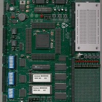
MPC555CME Freescale Semiconductor, MPC555CME Datasheet - Page 703

MPC555CME
Manufacturer Part Number
MPC555CME
Description
KIT EVALUATION FOR MPC555
Manufacturer
Freescale Semiconductor
Type
Microcontrollerr
Datasheet
1.MPC555CME.pdf
(966 pages)
Specifications of MPC555CME
Contents
Module Board, Installation Guide, Power Supply, Cable, Software and more
Processor To Be Evaluated
MPC555
Data Bus Width
32 bit
Interface Type
RS-232
For Use With/related Products
MPC555
Lead Free Status / RoHS Status
Contains lead / RoHS non-compliant
- Current page: 703 of 966
- Download datasheet (13Mb)
21.2.4.3 Detecting the Assertion/Negation of VSYNC
21.2.4.4 Detecting the Trace Window End Address
21.2.4.5 Compress
MPC555
USER’S MANUAL
VSYNC
VSYNC
VSYNC
Since the VF pins are used for reporting both instruction type information and queue
flush information, the external hardware must take special care when trying to detect
the assertion/negation of VSYNC. When VF = 011 it is a VSYNC assertion/negation
report only if the previous VF pins value was one of the following values: 000, 001, or
010.
The information on the status pins that describes the last fetched instruction and the
last queue/history buffer flushes, changes every clock. Cycles marked as program
trace cycle are generated on the external bus only when possible (when the SIU wins
the arbitration over the external bus). Therefore, there is some delay between the in-
formation reported on the status pins that a cycle marked as program trace cycle will
be performed on the external bus and the actual time that this cycle can be detected
on the external bus.
When VSYNC is negated by the user (through the serial interface of the development
port), the CPU delays the report of the of the assertion/negation of VSYNC on the VF
pins (VF = 011) until all addresses marked with the program trace cycle attribute were
visible externally. Therefore, the external hardware should stop sampling the value of
the status pins (VF and VFLS), and the address of the cycles marked as program trace
cycle immediately after the VSYNC report on the VF pins.
The last two instructions reported on the VF pins are not always valid. Therefore at the
last stage of the reconstruction software, the last two instructions should be ignored.
In order to store all the information generated on the pins during program trace (five
bits per clock + 30 bits per show cycle) a large memory buffer may be needed. How-
ever, since this information includes events that were canceled, compression can be
very effective. External hardware can be added to eliminate all canceled instructions
and report only on branches (taken and not taken), indirect flow change, and the num-
ber of sequential instructions after the last flow change.
VF1
011
011
011
/
MPC556
branch direct taken
branch indirect tak-
sequential
VF2
001
110
101
en
Table 21-4 Detecting the Trace Buffer Start Point
Starting point
offset (T1 - 4)
T1 - 4 +
DEVELOPMENT SUPPORT
T1
T2
Rev. 15 October 2000
VSYNC asserted followed by a sequential instruction. The
start address is T1
VSYNC asserted followed by a taken direct branch. The
start address is the target of the direct branch
VSYNC asserted followed by a taken indirect branch. The
start address is the target of the indirect branch
Description
MOTOROLA
21-7
Related parts for MPC555CME
Image
Part Number
Description
Manufacturer
Datasheet
Request
R

Part Number:
Description:
MPC555 Interrupts
Manufacturer:
Freescale Semiconductor / Motorola
Datasheet:
Part Number:
Description:
Manufacturer:
Freescale Semiconductor, Inc
Datasheet:
Part Number:
Description:
Manufacturer:
Freescale Semiconductor, Inc
Datasheet:
Part Number:
Description:
Manufacturer:
Freescale Semiconductor, Inc
Datasheet:
Part Number:
Description:
Manufacturer:
Freescale Semiconductor, Inc
Datasheet:
Part Number:
Description:
Manufacturer:
Freescale Semiconductor, Inc
Datasheet:
Part Number:
Description:
Manufacturer:
Freescale Semiconductor, Inc
Datasheet:
Part Number:
Description:
Manufacturer:
Freescale Semiconductor, Inc
Datasheet:
Part Number:
Description:
Manufacturer:
Freescale Semiconductor, Inc
Datasheet:
Part Number:
Description:
Manufacturer:
Freescale Semiconductor, Inc
Datasheet:
Part Number:
Description:
Manufacturer:
Freescale Semiconductor, Inc
Datasheet:
Part Number:
Description:
Manufacturer:
Freescale Semiconductor, Inc
Datasheet:
Part Number:
Description:
Manufacturer:
Freescale Semiconductor, Inc
Datasheet:
Part Number:
Description:
Manufacturer:
Freescale Semiconductor, Inc
Datasheet:
Part Number:
Description:
Manufacturer:
Freescale Semiconductor, Inc
Datasheet:


