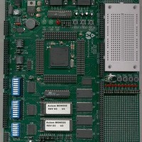
MPC555CME Freescale Semiconductor, MPC555CME Datasheet - Page 478

MPC555CME
Manufacturer Part Number
MPC555CME
Description
KIT EVALUATION FOR MPC555
Manufacturer
Freescale Semiconductor
Type
Microcontrollerr
Datasheet
1.MPC555CME.pdf
(966 pages)
Specifications of MPC555CME
Contents
Module Board, Installation Guide, Power Supply, Cable, Software and more
Processor To Be Evaluated
MPC555
Data Bus Width
32 bit
Interface Type
RS-232
For Use With/related Products
MPC555
Lead Free Status / RoHS Status
Contains lead / RoHS non-compliant
- Current page: 478 of 966
- Download datasheet (13Mb)
Access
14.7.1.1 QSPI Control Register 0
SPCR0 — QSPI Control Register 0
MPC555
USER’S MANUAL
RESET:
NOTES:
MSTR
MSB
S/U
S/U
S/U
S/U
S/U
S/U
S/U
1. S = Supervisor access only
2. 8-bit registers, such as SPCR3 and SPSR, are on 8-bit boundaries. 16-bit registers such as SPCR0 are on 16-bit
0
0
To ensure proper operation, set the QSPI enable bit (SPE) in SPCR1 only after initial-
izing the other control registers. Setting this bit starts the QSPI.
Rewriting the same value to a control register does not affect QSPI operation with the
exception of writing NEWQP in SPCR2. Rewriting the same value to these bits causes
the RAM queue pointer to restart execution at the designated location.
Before changing control bits, the user should halt the QSPI. Writing a different value
into a control register other than SPCR2 while the QSPI is enabled may disrupt oper-
ation. SPCR2 is buffered, preventing any disruption of the current serial transfer. After
the current serial transfer is completed, the new SPCR2 value becomes effective.
SPCR0 contains parameters for configuring the QSPI before it is enabled. The CPU
has read/write access to SPCR0, but the QSPI has read access only. SPCR0 must be
initialized before QSPI operation begins. Writing a new value to SPCR0 while the
QSPI is enabled disrupts operation.
S/U = Supervisor access only or unrestricted user access (assignable data space).
boundaries.
1
WOM
/
0x30 51C0 –
0x30 5140 –
0x30 5180 –
0x30 501E/
0x30 51DF
0x30 501A
0x30 501C
0x30 501F
0x30 517F
0x30 51BF
0x30 5018
Q
1
0
MPC556
Address
2
0
MSB
3
0
BITS
See
2
QSPI Control Register 3 (SPCR3)
QUEUED SERIAL MULTI-CHANNEL MODULE
4
0
Table 14-17
Table 14-12 QSPI Register Map
5
0
Rev. 15 October 2000
CPOL CPHA
for bit descriptions.
6
0
See
See
See
Transmit Data RAM (32 half-words)
Receive Data RAM (32 half-words)
QSPI Control Register 0 (SPCR0)
QSPI Control Register 1 (SPCR1)
QSPI Control Register 2 (SPCR2)
7
1
Table 14-13
Table 14-15
Table 14-16
Command RAM (32 bytes)
8
0
9
0
for bit descriptions.
for bit descriptions.
for bit descriptions.
See
10
0
QSPI Status Register (SPSR)
Table 14-18
11
0
SPBR
12
0
for bit descriptions.
13
1
0x30 5018
MOTOROLA
14
0
14-16
LSB
15
LSB
0
Related parts for MPC555CME
Image
Part Number
Description
Manufacturer
Datasheet
Request
R

Part Number:
Description:
MPC555 Interrupts
Manufacturer:
Freescale Semiconductor / Motorola
Datasheet:
Part Number:
Description:
Manufacturer:
Freescale Semiconductor, Inc
Datasheet:
Part Number:
Description:
Manufacturer:
Freescale Semiconductor, Inc
Datasheet:
Part Number:
Description:
Manufacturer:
Freescale Semiconductor, Inc
Datasheet:
Part Number:
Description:
Manufacturer:
Freescale Semiconductor, Inc
Datasheet:
Part Number:
Description:
Manufacturer:
Freescale Semiconductor, Inc
Datasheet:
Part Number:
Description:
Manufacturer:
Freescale Semiconductor, Inc
Datasheet:
Part Number:
Description:
Manufacturer:
Freescale Semiconductor, Inc
Datasheet:
Part Number:
Description:
Manufacturer:
Freescale Semiconductor, Inc
Datasheet:
Part Number:
Description:
Manufacturer:
Freescale Semiconductor, Inc
Datasheet:
Part Number:
Description:
Manufacturer:
Freescale Semiconductor, Inc
Datasheet:
Part Number:
Description:
Manufacturer:
Freescale Semiconductor, Inc
Datasheet:
Part Number:
Description:
Manufacturer:
Freescale Semiconductor, Inc
Datasheet:
Part Number:
Description:
Manufacturer:
Freescale Semiconductor, Inc
Datasheet:
Part Number:
Description:
Manufacturer:
Freescale Semiconductor, Inc
Datasheet:


