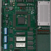
MPC555CME Freescale Semiconductor, MPC555CME Datasheet - Page 332

MPC555CME
Manufacturer Part Number
MPC555CME
Description
KIT EVALUATION FOR MPC555
Manufacturer
Freescale Semiconductor
Type
Microcontrollerr
Datasheet
1.MPC555CME.pdf
(966 pages)
Specifications of MPC555CME
Contents
Module Board, Installation Guide, Power Supply, Cable, Software and more
Processor To Be Evaluated
MPC555
Data Bus Width
32 bit
Interface Type
RS-232
For Use With/related Products
MPC555
Lead Free Status / RoHS Status
Contains lead / RoHS non-compliant
- Current page: 332 of 966
- Download datasheet (13Mb)
9.5.7.1 Transfer Start
9.5.7.2 Address Bus
9.5.7.3 Read/Write
9.5.7.4 Burst Indicator
MPC555
USER’S MANUAL
This signal (TS) indicates the beginning of a transaction on the bus addressing a slave
device. This signal should be asserted by a master only after the ownership of the bus
was granted by the arbitration protocol. This signal is asserted for the first cycle of the
transaction only and is negated in successive clock cycles until the end of the trans-
action. The master should three-state this signal when it relinquishes the bus to avoid
contention between two or more masters in this line. This situation indicates that an
external pull-up resistor should be connected to the TS signal to avoid having a slave
recognize this signal as asserted when no master drives it. Refer to
The address bus consists of 32 bits, with ADDR[0] the most significant bit and AD-
DR[31] the least significant bit. The bus is byte-addressable, so each address can ad-
dress one or more bytes. The address and its attributes are driven on the bus with the
transfer start signal and kept valid until the bus master receives the transfer acknowl-
edge signal from the slave. To distinguish the individual byte, the slave device must
observe the TSIZ signals.
A high value on the RD/WR line indicates a read access. A low value indicates a write
access.
BURST is driven by the bus master at the beginning of the bus cycle along with the
address to indicate that the transfer is a burst transfer.
The MPC555 / MPC556 supports a non-wrapping, four-beat maximum, critical word
first burst type. The maximum burst size is 16 bytes. For a 32-bit port, the burst in-
cludes four beats. For a 16-bit port, the burst includes 8 beats. For an 8-bit port, the
burst includes 16 beats at most. Note that 8- and 16-bit ports must be controlled by the
memory controller.
The actual size of the burst is determined by the address of the starting word of the
burst. Refer to
ADDR[28:29]
Address
Starting
00
01
10
11
/
MPC556
word 1 → word 2 → word 3
Burst Order (Assuming
Table 9-5
word 0 → word 1 →
32-bit Port Size)
word 2 → word 3
word 2 → word 3
word 3
Table 9-5 Burst Length and Order
and
EXTERNAL BUS INTERFACE
Table
Rev. 15 October 2000
Burst Length in
Words (Beats)
9-6.
4
3
2
1
Burst Length
in Bytes
16
12
8
4
BDIP never asserted
Comments
Figure
MOTOROLA
9-24.
9-36
Related parts for MPC555CME
Image
Part Number
Description
Manufacturer
Datasheet
Request
R

Part Number:
Description:
MPC555 Interrupts
Manufacturer:
Freescale Semiconductor / Motorola
Datasheet:
Part Number:
Description:
Manufacturer:
Freescale Semiconductor, Inc
Datasheet:
Part Number:
Description:
Manufacturer:
Freescale Semiconductor, Inc
Datasheet:
Part Number:
Description:
Manufacturer:
Freescale Semiconductor, Inc
Datasheet:
Part Number:
Description:
Manufacturer:
Freescale Semiconductor, Inc
Datasheet:
Part Number:
Description:
Manufacturer:
Freescale Semiconductor, Inc
Datasheet:
Part Number:
Description:
Manufacturer:
Freescale Semiconductor, Inc
Datasheet:
Part Number:
Description:
Manufacturer:
Freescale Semiconductor, Inc
Datasheet:
Part Number:
Description:
Manufacturer:
Freescale Semiconductor, Inc
Datasheet:
Part Number:
Description:
Manufacturer:
Freescale Semiconductor, Inc
Datasheet:
Part Number:
Description:
Manufacturer:
Freescale Semiconductor, Inc
Datasheet:
Part Number:
Description:
Manufacturer:
Freescale Semiconductor, Inc
Datasheet:
Part Number:
Description:
Manufacturer:
Freescale Semiconductor, Inc
Datasheet:
Part Number:
Description:
Manufacturer:
Freescale Semiconductor, Inc
Datasheet:
Part Number:
Description:
Manufacturer:
Freescale Semiconductor, Inc
Datasheet:


