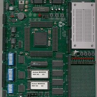
MPC555CME Freescale Semiconductor, MPC555CME Datasheet - Page 682

MPC555CME
Manufacturer Part Number
MPC555CME
Description
KIT EVALUATION FOR MPC555
Manufacturer
Freescale Semiconductor
Type
Microcontrollerr
Datasheet
1.MPC555CME.pdf
(966 pages)
Specifications of MPC555CME
Contents
Module Board, Installation Guide, Power Supply, Cable, Software and more
Processor To Be Evaluated
MPC555
Data Bus Width
32 bit
Interface Type
RS-232
For Use With/related Products
MPC555
Lead Free Status / RoHS Status
Contains lead / RoHS non-compliant
- Current page: 682 of 966
- Download datasheet (13Mb)
19.7.7 Starting and Ending a Program or Erase Sequence
MPC555
USER’S MANUAL
In this example system clock frequency = 40 MHz; the system clock period is therefore
25 ns.
The SES bit is used to signal the start and end of a program or erase sequence. At the
start of a program or erase sequence, SES is set (written to a one). This locks
PROTECT[0:7], SCLKR[0:2], CLKPE[0:1], CLKPM[0:6], BLOCK[0:7], CSC and PE. If
PE = 0 and SES = 1, SIE is write-locked. At this point the CMF EEPROM is ready to
receive either the programming writes or the erase interlock write.
If the PE bit is a zero, the CMF BIU accepts programming writes to the CMF array ad-
dress for programming. The first programming write selects the program page offset
address (ADDR[17:25]) to be programmed along with the data for the programming
buffers at the location written. All programming writes after the first will update the pro-
gram buffers using the lower address (ADDR[26:29]) and the block address (AD-
DR[14:16]) to select the program page buffers to receive the data. For further
information see section
ten to the program buffers the EHV bit is set (written to a one) to start the programming
pulse and lock out further programming writes.
If the PE bit = 1, the CMF BIU accepts writes to any CMF array address as an erase-
interlock write. An erase interlock write is required before the EHV bit can be set.
At the end of the program or erase operation the SES bit must be cleared (written to a
zero) to return to normal operation and release the program buffers, PROTECT[0:7],
SCLKR[0:2], CLKPE[0:1], CLKPM[0:6], BLOCK[0:7], CSC and PE.
The default reset state of SES is not configured for program or erase operation (SES
= 0).
1. Determine SCLKR:
2. Determine CLKPE:
3. Determine CLKPM:
4. Check the results:
/
MPC556
From
From
ponents in the range of N = 5, 6, 7, or 8. While any of these values can be se-
lected CLKPE[0:1] = 0b00, N = 5, will be used for the example.
Using the selected values of N and R in the pulse width equation and solving
for M yields M = 8. Therefore, CLKPM[0:6] = 0x7 (0b0000111).
Pulse Width = System Clock Period
Using SCLKR[0:2] = 0b101, CLKPE[0:1] = 0b00, CLKPM[0:6] = 0b0000111
and PE = 0 at 40 MHz system clock. Pulse Width = 25 ns • 4 • 2
program pulse.
The erase interlock write is a write to any CMF EEPROM array loca-
tion after SES is set and PE = 1.
Table 19-12
Table 19-13
19.2.2.2 Program Page
a 40 MHz system clock uses SCLKR[0:2] = 0b101, R = 4.
a 25.6 µs program pulse, PE = 0, can be generated by ex-
CDR MoneT FLASH EEPROM
Rev. 15 October 2000
NOTE
•
R
•
Buffers. After the data has been writ-
2
N
•
M
5
• 8 = 25.6 µs
MOTOROLA
19-30
Related parts for MPC555CME
Image
Part Number
Description
Manufacturer
Datasheet
Request
R

Part Number:
Description:
MPC555 Interrupts
Manufacturer:
Freescale Semiconductor / Motorola
Datasheet:
Part Number:
Description:
Manufacturer:
Freescale Semiconductor, Inc
Datasheet:
Part Number:
Description:
Manufacturer:
Freescale Semiconductor, Inc
Datasheet:
Part Number:
Description:
Manufacturer:
Freescale Semiconductor, Inc
Datasheet:
Part Number:
Description:
Manufacturer:
Freescale Semiconductor, Inc
Datasheet:
Part Number:
Description:
Manufacturer:
Freescale Semiconductor, Inc
Datasheet:
Part Number:
Description:
Manufacturer:
Freescale Semiconductor, Inc
Datasheet:
Part Number:
Description:
Manufacturer:
Freescale Semiconductor, Inc
Datasheet:
Part Number:
Description:
Manufacturer:
Freescale Semiconductor, Inc
Datasheet:
Part Number:
Description:
Manufacturer:
Freescale Semiconductor, Inc
Datasheet:
Part Number:
Description:
Manufacturer:
Freescale Semiconductor, Inc
Datasheet:
Part Number:
Description:
Manufacturer:
Freescale Semiconductor, Inc
Datasheet:
Part Number:
Description:
Manufacturer:
Freescale Semiconductor, Inc
Datasheet:
Part Number:
Description:
Manufacturer:
Freescale Semiconductor, Inc
Datasheet:
Part Number:
Description:
Manufacturer:
Freescale Semiconductor, Inc
Datasheet:


