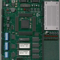
MPC555CME Freescale Semiconductor, MPC555CME Datasheet - Page 676

MPC555CME
Manufacturer Part Number
MPC555CME
Description
KIT EVALUATION FOR MPC555
Manufacturer
Freescale Semiconductor
Type
Microcontrollerr
Datasheet
1.MPC555CME.pdf
(966 pages)
Specifications of MPC555CME
Contents
Module Board, Installation Guide, Power Supply, Cable, Software and more
Processor To Be Evaluated
MPC555
Data Bus Width
32 bit
Interface Type
RS-232
For Use With/related Products
MPC555
Lead Free Status / RoHS Status
Contains lead / RoHS non-compliant
- Current page: 676 of 966
- Download datasheet (13Mb)
MPC555
USER’S MANUAL
10.
4. Execute an erase interlock write to any CMF array location.
5. Write EHV = 1 in the CMFCTL register.
6. Read the CMFCTL register until HVS = 0.
7. Write EHV = 0 in the CMFCTL register.
8. To verify the erase operation, read all locations that are being erased, including
9. To reduce the time used for erase margin reads, upon the first read of a zero,
/
MPC556
a. Write new pulse width parameters, SCLKR, CLKPE, and CLKPM (if
b. Write new PAWS value (if required per
c. Write new values for NVR and GDB (if required per
d. Go back to step 5 to apply additional erase pulses.
pulse width bit settings per
the shadow information if the block containing it is erased. Off-page reads are
erase margin reads that update the read page buffer. (See section
Erase Margin
do the following:
Write SES = 0 in the CMFCTL register.
required per
Do not perform erase margin reads until reaching the condition
PAWS=0b111, NVR=0 and GDB=1.
After a location has been verified (all bits erased), it is not necessary
to verify the location after subsequent erase pulses.
Reads.) If all the locations read as erased, go to step 9.
Table
CDR MoneT FLASH EEPROM
19-5).
Rev. 15 October 2000
Table
19-5.
NOTE
NOTE
Table
19-5).
Table
19-5).
MOTOROLA
19.6.2
19-24
Related parts for MPC555CME
Image
Part Number
Description
Manufacturer
Datasheet
Request
R

Part Number:
Description:
MPC555 Interrupts
Manufacturer:
Freescale Semiconductor / Motorola
Datasheet:
Part Number:
Description:
Manufacturer:
Freescale Semiconductor, Inc
Datasheet:
Part Number:
Description:
Manufacturer:
Freescale Semiconductor, Inc
Datasheet:
Part Number:
Description:
Manufacturer:
Freescale Semiconductor, Inc
Datasheet:
Part Number:
Description:
Manufacturer:
Freescale Semiconductor, Inc
Datasheet:
Part Number:
Description:
Manufacturer:
Freescale Semiconductor, Inc
Datasheet:
Part Number:
Description:
Manufacturer:
Freescale Semiconductor, Inc
Datasheet:
Part Number:
Description:
Manufacturer:
Freescale Semiconductor, Inc
Datasheet:
Part Number:
Description:
Manufacturer:
Freescale Semiconductor, Inc
Datasheet:
Part Number:
Description:
Manufacturer:
Freescale Semiconductor, Inc
Datasheet:
Part Number:
Description:
Manufacturer:
Freescale Semiconductor, Inc
Datasheet:
Part Number:
Description:
Manufacturer:
Freescale Semiconductor, Inc
Datasheet:
Part Number:
Description:
Manufacturer:
Freescale Semiconductor, Inc
Datasheet:
Part Number:
Description:
Manufacturer:
Freescale Semiconductor, Inc
Datasheet:
Part Number:
Description:
Manufacturer:
Freescale Semiconductor, Inc
Datasheet:


