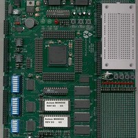
MPC555CME Freescale Semiconductor, MPC555CME Datasheet - Page 354

MPC555CME
Manufacturer Part Number
MPC555CME
Description
KIT EVALUATION FOR MPC555
Manufacturer
Freescale Semiconductor
Type
Microcontrollerr
Datasheet
1.MPC555CME.pdf
(966 pages)
Specifications of MPC555CME
Contents
Module Board, Installation Guide, Power Supply, Cable, Software and more
Processor To Be Evaluated
MPC555
Data Bus Width
32 bit
Interface Type
RS-232
For Use With/related Products
MPC555
Lead Free Status / RoHS Status
Contains lead / RoHS non-compliant
- Current page: 354 of 966
- Download datasheet (13Mb)
MPC555
USER’S MANUAL
chip-select for accessing the boot flash EEPROM. The chip select allows zero to 30
wait states.
Figure 10-2
Most memory controller features are common to all four banks. (For features unique
to the CS[0] bank, refer to
address decode for each memory bank is possible with 17 bits having address mask-
ing. The full 32-bit decode is available, even if all 32 address bits are not sent to the
MPC555 / MPC556 pins.
Each memory bank includes a variable block size of 32 Kbytes, 64 Kbytes and up to
4 Gbytes. Each memory bank can be selected for read-only or read/write operation.
The access to a memory bank can be restricted to certain address type codes for sys-
tem protection. The address type comparison occurs with a mask option as well.
INTERNAL ADDRESSES [0:16, AT[0:2]
Base
Register
/
MPC556
Base Register 3 (BR3)
is a block diagram of the MPC555 / MPC556 memory controller.
Base Register (DMBR)
Figure 10-2 Memory Controller Block Diagram
Dual Mapping
Region Match Logic
10.4 Global (Boot) Chip-Select
0 (OR0)
MEMORY CONTROLLER
1 (OR1)
Rev. 15 October 2000
2 (OR2)
Option
Register
Wait State
Counter
Option Register 3 (OR3)
Option Register (DMOR)
Dual Mapping
Expired
Load
ATTRIBUTES
0 (OR0)
Operation.) A full 32-bit
1 (OR1)
General-Purpose
2 (OR2)
Chip-Select
Machine
(GPCM)
MOTOROLA
CS[0:3]
WE/BE[0:3]
OE
10-2
Related parts for MPC555CME
Image
Part Number
Description
Manufacturer
Datasheet
Request
R

Part Number:
Description:
MPC555 Interrupts
Manufacturer:
Freescale Semiconductor / Motorola
Datasheet:
Part Number:
Description:
Manufacturer:
Freescale Semiconductor, Inc
Datasheet:
Part Number:
Description:
Manufacturer:
Freescale Semiconductor, Inc
Datasheet:
Part Number:
Description:
Manufacturer:
Freescale Semiconductor, Inc
Datasheet:
Part Number:
Description:
Manufacturer:
Freescale Semiconductor, Inc
Datasheet:
Part Number:
Description:
Manufacturer:
Freescale Semiconductor, Inc
Datasheet:
Part Number:
Description:
Manufacturer:
Freescale Semiconductor, Inc
Datasheet:
Part Number:
Description:
Manufacturer:
Freescale Semiconductor, Inc
Datasheet:
Part Number:
Description:
Manufacturer:
Freescale Semiconductor, Inc
Datasheet:
Part Number:
Description:
Manufacturer:
Freescale Semiconductor, Inc
Datasheet:
Part Number:
Description:
Manufacturer:
Freescale Semiconductor, Inc
Datasheet:
Part Number:
Description:
Manufacturer:
Freescale Semiconductor, Inc
Datasheet:
Part Number:
Description:
Manufacturer:
Freescale Semiconductor, Inc
Datasheet:
Part Number:
Description:
Manufacturer:
Freescale Semiconductor, Inc
Datasheet:
Part Number:
Description:
Manufacturer:
Freescale Semiconductor, Inc
Datasheet:


