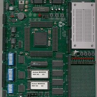
MPC555CME Freescale Semiconductor, MPC555CME Datasheet - Page 285

MPC555CME
Manufacturer Part Number
MPC555CME
Description
KIT EVALUATION FOR MPC555
Manufacturer
Freescale Semiconductor
Type
Microcontrollerr
Datasheet
1.MPC555CME.pdf
(966 pages)
Specifications of MPC555CME
Contents
Module Board, Installation Guide, Power Supply, Cable, Software and more
Processor To Be Evaluated
MPC555
Data Bus Width
32 bit
Interface Type
RS-232
For Use With/related Products
MPC555
Lead Free Status / RoHS Status
Contains lead / RoHS non-compliant
- Current page: 285 of 966
- Download datasheet (13Mb)
8.10 VDDSRAM Supply Failure Detection
8.11 Power Up/Down Sequencing
MPC555
USER’S MANUAL
SPR 268, 269,
SPR Number
Address or
284, 285,
SPR 22
Figure 8-12
WR.
A special circuit for VDDSRAM supply failure detection is provided. In the case of sup-
ply failure detection, the dedicated sticky bits LVSRS in the VSRMCR register are as-
serted. Software can read or clear these bits. The user should enable the detector and
then clear these bits. If the user reads any of the LVSR bits as one, then a power failure
of VDDSRAM has occurred. The circuit is capable of detecting supply failure below 2.6
V. Also, enable/disable control bit for the VDDSRAM detector may be used to discon-
nect the circuit and save the detector power consumption.
Figure 8-13
during normal operation. Note that for each of the conditions detailing the voltage re-
lationships the absolute bounds of the minimum and maximum voltage supply cannot
be violated, i.e. the value of VDDL cannot fall below 3.0 V or exceed 3.6 V and the
value of VDDH cannot fall below 4.5 V or exceed 5.5 V for normal operation. Further
information detailing the functionality of the VPP signal for flash program and erase is
outlined in
tion during power up sequencing can not be specified prior to evaluation and charac-
/
Write to the key other value
MPC556
(Valid for other registers)
Table 8-8 KAPWR Registers and Key Registers (Continued)
Decrementer
See
for bit descriptions.
Time Base
See
scriptions.
19.9.2 FLASH Program/Erase Voltage
KAPWR Register
illustrates the process of locking or unlocking a register powered by KAP-
Power On Reset
and
Figure 8-12 Keep Alive Register Key State Diagram
3.9.5 Decrementer Register (DEC)
Table 3-11
Figure 8-14
and
Register
Table 3-14
CLOCKS AND POWER CONTROL
detail the power-up sequencing for MPC555 / MPC556
Rev. 15 October 2000
for bit de-
Locked
Open
0x2F C30C
Address
Conditioning. Power consump-
Time Base and Decrementer Key (TBK)
Associated Key Register
Write to the Key 0x55CCAA33
(Valid for RTC, RTSEC,
RTCAL and RTCSC)
Power On Reset
Register
MOTOROLA
8-25
Related parts for MPC555CME
Image
Part Number
Description
Manufacturer
Datasheet
Request
R

Part Number:
Description:
MPC555 Interrupts
Manufacturer:
Freescale Semiconductor / Motorola
Datasheet:
Part Number:
Description:
Manufacturer:
Freescale Semiconductor, Inc
Datasheet:
Part Number:
Description:
Manufacturer:
Freescale Semiconductor, Inc
Datasheet:
Part Number:
Description:
Manufacturer:
Freescale Semiconductor, Inc
Datasheet:
Part Number:
Description:
Manufacturer:
Freescale Semiconductor, Inc
Datasheet:
Part Number:
Description:
Manufacturer:
Freescale Semiconductor, Inc
Datasheet:
Part Number:
Description:
Manufacturer:
Freescale Semiconductor, Inc
Datasheet:
Part Number:
Description:
Manufacturer:
Freescale Semiconductor, Inc
Datasheet:
Part Number:
Description:
Manufacturer:
Freescale Semiconductor, Inc
Datasheet:
Part Number:
Description:
Manufacturer:
Freescale Semiconductor, Inc
Datasheet:
Part Number:
Description:
Manufacturer:
Freescale Semiconductor, Inc
Datasheet:
Part Number:
Description:
Manufacturer:
Freescale Semiconductor, Inc
Datasheet:
Part Number:
Description:
Manufacturer:
Freescale Semiconductor, Inc
Datasheet:
Part Number:
Description:
Manufacturer:
Freescale Semiconductor, Inc
Datasheet:
Part Number:
Description:
Manufacturer:
Freescale Semiconductor, Inc
Datasheet:


