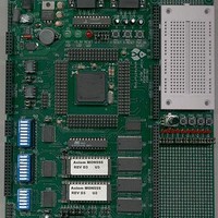
MPC555CME Freescale Semiconductor, MPC555CME Datasheet - Page 77

MPC555CME
Manufacturer Part Number
MPC555CME
Description
KIT EVALUATION FOR MPC555
Manufacturer
Freescale Semiconductor
Type
Microcontrollerr
Datasheet
1.MPC555CME.pdf
(966 pages)
Specifications of MPC555CME
Contents
Module Board, Installation Guide, Power Supply, Cable, Software and more
Processor To Be Evaluated
MPC555
Data Bus Width
32 bit
Interface Type
RS-232
For Use With/related Products
MPC555
Lead Free Status / RoHS Status
Contains lead / RoHS non-compliant
- Current page: 77 of 966
- Download datasheet (13Mb)
2.3.1.30 IWP[0:1]/VFLS[0:1]
2.3.1.31 TMS
2.3.1.32 TDI/DSDI
2.3.1.33 TCK/DSCK
2.3.1.34 TDO/DSDO
MPC555
USER’S MANUAL
Bus Busy – Indicates that the master is using the bus. This pin is an active negate
signal and may need an external pull-up resistor to ensure proper operation and signal
timing specifications.
Visible Instruction Queue Flush Status – This output line together with VF0 and VF1
is output by the chip when a program instructions flow tracking is required by the user.
VF report the number of instructions flushed from the instruction queue in the internal
core.
Instruction Watchpoint 3 – This output line reports the detection of an instruction
watchpoint in the program flow executed by the internal core.
Pin Name: iwp0_vfls0 - iwp1_vfls1 (2 pins)
Instruction Watchpoint – These output lines report the detection of an instruction
watchpoint in the program flow executed by the RCPU.
Visible History Buffer Flush Status – These signals are output by the chip to enable
program instruction flow tracking. They report the number of instructions flushed from
the history buffer in the RCPU. See
tails.
Pin Name: tms
Test Mode Select – This input controls test mode operations for on-board test logic
(JTAG).
Pin Name: tdi_dsdi
Test Data In – This input is used for serial test instructions and test data for on-board
test logic (JTAG).
Development Serial Data Input – This input line is the data in for the debug port in-
terface. See
Pin Name: tck_dsck
Test Clock – This input provides a clock for on-board test logic (JTAG).
Development Serial Clock – This input line is the clock for the debug port interface.
See
Pin Name: tdo_dsdo
/
SECTION 21 DEVELOPMENT SUPPORT
MPC556
SECTION 21 DEVELOPMENT SUPPORT
SIGNAL DESCRIPTIONS
Rev. 15 October 2000
SECTION 21 DEVELOPMENT SUPPORT
for details.
for details.
MOTOROLA
for de-
2-19
Related parts for MPC555CME
Image
Part Number
Description
Manufacturer
Datasheet
Request
R

Part Number:
Description:
MPC555 Interrupts
Manufacturer:
Freescale Semiconductor / Motorola
Datasheet:
Part Number:
Description:
Manufacturer:
Freescale Semiconductor, Inc
Datasheet:
Part Number:
Description:
Manufacturer:
Freescale Semiconductor, Inc
Datasheet:
Part Number:
Description:
Manufacturer:
Freescale Semiconductor, Inc
Datasheet:
Part Number:
Description:
Manufacturer:
Freescale Semiconductor, Inc
Datasheet:
Part Number:
Description:
Manufacturer:
Freescale Semiconductor, Inc
Datasheet:
Part Number:
Description:
Manufacturer:
Freescale Semiconductor, Inc
Datasheet:
Part Number:
Description:
Manufacturer:
Freescale Semiconductor, Inc
Datasheet:
Part Number:
Description:
Manufacturer:
Freescale Semiconductor, Inc
Datasheet:
Part Number:
Description:
Manufacturer:
Freescale Semiconductor, Inc
Datasheet:
Part Number:
Description:
Manufacturer:
Freescale Semiconductor, Inc
Datasheet:
Part Number:
Description:
Manufacturer:
Freescale Semiconductor, Inc
Datasheet:
Part Number:
Description:
Manufacturer:
Freescale Semiconductor, Inc
Datasheet:
Part Number:
Description:
Manufacturer:
Freescale Semiconductor, Inc
Datasheet:
Part Number:
Description:
Manufacturer:
Freescale Semiconductor, Inc
Datasheet:


