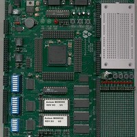
MPC555CME Freescale Semiconductor, MPC555CME Datasheet - Page 680

MPC555CME
Manufacturer Part Number
MPC555CME
Description
KIT EVALUATION FOR MPC555
Manufacturer
Freescale Semiconductor
Type
Microcontrollerr
Datasheet
1.MPC555CME.pdf
(966 pages)
Specifications of MPC555CME
Contents
Module Board, Installation Guide, Power Supply, Cable, Software and more
Processor To Be Evaluated
MPC555
Data Bus Width
32 bit
Interface Type
RS-232
For Use With/related Products
MPC555
Lead Free Status / RoHS Status
Contains lead / RoHS non-compliant
- Current page: 680 of 966
- Download datasheet (13Mb)
19.7.3 System Clock Scaling
MPC555
USER’S MANUAL
The following subsections explain how the values for R, N, and M are determined.
The first term of the pulse width timing equation is the clock scaling, R. The value of R
is determined by the system clock range (SCLKR) field. SCLKR defines the pulse tim-
er’s base clock using the system clock. Use
the system clock frequency. The system clock period is multiplied by the clock scaling
value to generate a 83.3-ns to 125-ns scaled clock. This scaled clock is used to run
the charge pump submodule and the next functional block of the timing control.
SCLKR[0:2]
110 and 111
/
MPC556
000
001
010
011
100
101
Where:
The minimum specified system clock frequency for performing pro-
gram and erase operations is 8.0 MHz. The CMF EEPROM does not
have any means to monitor the system clock frequency and will not
prevent program or erase operation at frequencies below 8.0 MHz.
Attempting to program or erase the CMF EEPROM at system clock
frequencies lower than 8.0 MHz will not damage the device if the
maximum pulse times and total times are not exceeded. While some
bits in the CMF EEPROM array may change state if programmed or
erased at system clock frequencies below 8.0 MHz, the full program
or erase transition is not ensured.
Never stop the U-bus clock or alter its frequency during a program or
erase operation. Changing the clock frequency during a program or
erase operation results in inaccurate pulse widths and variations in
the charge pump output. This includes loss of system clock/PLL.
R = Clock Scaling
N = 5 + CLKPE[0:1] + ((PE | CSC)
M = 1 + CLKPM[0:6]
Not for customer use.
not specified and pulse is not terminated by the timer con-
Pulse Width = System Clock Period
trol. Recovery time is specified to be 128 clocks.
Table 19-12 System Clock Range
Minimum
CDR MoneT FLASH EEPROM
System Clock Frequency (MHz)
12
18
24
36
8
Rev. 15 October 2000
Program and erase timing control
Reserved by Motorola for future use
WARNING
NOTE
Table 19-12
Maximum
12
18
24
36
40
•
10)
•
R
to set SCLKR based upon
•
2
N
•
M
Clock Scaling (R)
3/2
1
1
2
3
4
MOTOROLA
19-28
Related parts for MPC555CME
Image
Part Number
Description
Manufacturer
Datasheet
Request
R

Part Number:
Description:
MPC555 Interrupts
Manufacturer:
Freescale Semiconductor / Motorola
Datasheet:
Part Number:
Description:
Manufacturer:
Freescale Semiconductor, Inc
Datasheet:
Part Number:
Description:
Manufacturer:
Freescale Semiconductor, Inc
Datasheet:
Part Number:
Description:
Manufacturer:
Freescale Semiconductor, Inc
Datasheet:
Part Number:
Description:
Manufacturer:
Freescale Semiconductor, Inc
Datasheet:
Part Number:
Description:
Manufacturer:
Freescale Semiconductor, Inc
Datasheet:
Part Number:
Description:
Manufacturer:
Freescale Semiconductor, Inc
Datasheet:
Part Number:
Description:
Manufacturer:
Freescale Semiconductor, Inc
Datasheet:
Part Number:
Description:
Manufacturer:
Freescale Semiconductor, Inc
Datasheet:
Part Number:
Description:
Manufacturer:
Freescale Semiconductor, Inc
Datasheet:
Part Number:
Description:
Manufacturer:
Freescale Semiconductor, Inc
Datasheet:
Part Number:
Description:
Manufacturer:
Freescale Semiconductor, Inc
Datasheet:
Part Number:
Description:
Manufacturer:
Freescale Semiconductor, Inc
Datasheet:
Part Number:
Description:
Manufacturer:
Freescale Semiconductor, Inc
Datasheet:
Part Number:
Description:
Manufacturer:
Freescale Semiconductor, Inc
Datasheet:


