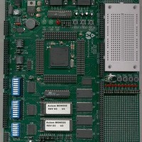
MPC555CME Freescale Semiconductor, MPC555CME Datasheet - Page 658

MPC555CME
Manufacturer Part Number
MPC555CME
Description
KIT EVALUATION FOR MPC555
Manufacturer
Freescale Semiconductor
Type
Microcontrollerr
Datasheet
1.MPC555CME.pdf
(966 pages)
Specifications of MPC555CME
Contents
Module Board, Installation Guide, Power Supply, Cable, Software and more
Processor To Be Evaluated
MPC555
Data Bus Width
32 bit
Interface Type
RS-232
For Use With/related Products
MPC555
Lead Free Status / RoHS Status
Contains lead / RoHS non-compliant
- Current page: 658 of 966
- Download datasheet (13Mb)
MPC555
USER’S MANUAL
Bit(s)
8:15
1:2
6:7
0
3
4
5
SUPV[0:7]
/
CENSOR
ACCESS
MPC556
Name
LOCK
FIC
SIE
—
Lock control. When the LOCK control bit is cleared, the following bits are locked: FIC,
SUPV[0:7], DATA[0:7] and PROTECT[0:7]. Writes to these bits will have no effect.
In normal operation, once the LOCK bit is cleared, the write-lock can only be disabled again by
a master reset. The LOCK bit is writable if the device is in background debug mode and CSC = 0.
0 = Write-locked registers are protected
1 = Write-lock is disabled (reset state)
Warning:
are cleared, the device must use background debug mode to program or erase the CMF array.
Reserved
Force information censorship for access development. Refer to
sored Accesses
The FIC bit is write protected by the LOCK. If FIC = 1 it cannot be cleared except by a hard reset.
0 = Normal CMF censorship operation
1 = Forces the CMF into information censorship mode, unless ACCESS = 1
Shadow information enable. Refer to
The SIE bit is write protected by the SES bit for programming operation. Writes have no effect
if (SES = 1 and PE = 0). The SIE bit can be read whenever the registers are enabled.
0 = Normal array access
1 = Disables normal array access and selects the shadow information
Enable uncensored access. Refer to
Writes to this bit have no effect when CSC = 1. This bit can be set only when the MCU is in un-
censored mode.
0 = Censored CMF array access allowed only if the CMF censorship is no censorship, (FIC = 0
1 = Allows all CMF array access.
Censor accesses. The value of these bits is determined by the state of two NVM bits in two spe-
cial NVM fuses. Refer to
The default reset state of CENSOR is user defined by the FLASH NVM register bits.
00 = Cleared censorship, CMF array access allowed only if device is in uncensored mode or
01 = No censorship, All CMF array accesses allowed
10 = No censorship, All CMF array accesses allowed
11 = Information censorship, CMF array access allowed only if device is in uncensored mode or
Supervisor space. Each array block can be mapped into supervisor or unrestricted address
space. When an array block is mapped into supervisor address space, only supervisor accesses
are allowed. A user access to a location in supervisor address space will result in a data error
exception. When an array block is mapped into unrestricted address space, both supervisor and
user accesses are allowed.
The SUPV[0:7] bits are write protected by the LOCK and CSC bits. Writes will have no effect if
LOCK=0 or CSC=1.
0 = Array block M is placed in unrestricted address space
1 = Array block M is placed in supervisor address space (reset value)
and CENSOR[0] ≠ CENSOR[1])
ACCESS = 1
ACCESS = 1
Table 19-2 CMFMCR Bit Descriptions
If the lock protection mechanism is enabled (LOCK = 0) before the PROTECT[0:7] bits
for details.
CDR MoneT FLASH EEPROM
Rev. 15 October 2000
19.8 Censored and Non-Censored Accesses
19.8 Censored and Non-Censored Accesses
19.3 Shadow Information
Description
19.8 Censored and Non-Cen-
for details.
for details.
MOTOROLA
for details.
19-6
Related parts for MPC555CME
Image
Part Number
Description
Manufacturer
Datasheet
Request
R

Part Number:
Description:
MPC555 Interrupts
Manufacturer:
Freescale Semiconductor / Motorola
Datasheet:
Part Number:
Description:
Manufacturer:
Freescale Semiconductor, Inc
Datasheet:
Part Number:
Description:
Manufacturer:
Freescale Semiconductor, Inc
Datasheet:
Part Number:
Description:
Manufacturer:
Freescale Semiconductor, Inc
Datasheet:
Part Number:
Description:
Manufacturer:
Freescale Semiconductor, Inc
Datasheet:
Part Number:
Description:
Manufacturer:
Freescale Semiconductor, Inc
Datasheet:
Part Number:
Description:
Manufacturer:
Freescale Semiconductor, Inc
Datasheet:
Part Number:
Description:
Manufacturer:
Freescale Semiconductor, Inc
Datasheet:
Part Number:
Description:
Manufacturer:
Freescale Semiconductor, Inc
Datasheet:
Part Number:
Description:
Manufacturer:
Freescale Semiconductor, Inc
Datasheet:
Part Number:
Description:
Manufacturer:
Freescale Semiconductor, Inc
Datasheet:
Part Number:
Description:
Manufacturer:
Freescale Semiconductor, Inc
Datasheet:
Part Number:
Description:
Manufacturer:
Freescale Semiconductor, Inc
Datasheet:
Part Number:
Description:
Manufacturer:
Freescale Semiconductor, Inc
Datasheet:
Part Number:
Description:
Manufacturer:
Freescale Semiconductor, Inc
Datasheet:


