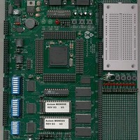
MPC555CME Freescale Semiconductor, MPC555CME Datasheet - Page 694

MPC555CME
Manufacturer Part Number
MPC555CME
Description
KIT EVALUATION FOR MPC555
Manufacturer
Freescale Semiconductor
Type
Microcontrollerr
Datasheet
1.MPC555CME.pdf
(966 pages)
Specifications of MPC555CME
Contents
Module Board, Installation Guide, Power Supply, Cable, Software and more
Processor To Be Evaluated
MPC555
Data Bus Width
32 bit
Interface Type
RS-232
For Use With/related Products
MPC555
Lead Free Status / RoHS Status
Contains lead / RoHS non-compliant
- Current page: 694 of 966
- Download datasheet (13Mb)
20.3 Programming Model
20.3.1 SRAM Module Configuration Register (SRAMMCR)
MPC555
USER’S MANUAL
The SRAM modules consist of two separately addressable sections the array itself,
and a set of registers used for configuration and testing of the SRAM array. The reg-
isters are located in the SRAM control register block, shown in
Figure 1-3
The control block for each of the two SRAM modules contains one control register for
configuring the array and one control register for use in testing.
Each SRAM module configuration register contains bits for setting access rights to the
array.
/
MPC556
Table 20-1
for the entire MPC555 / MPC556 memory map.
0x38 0000
0x38 0004
0x38 0008
0x38 000C
0x3F 8000
0x3F 8FFF
0x3F 9000
0x3F 97FF
0x3F 9800
0x3F 9FFF
0x3F A000
0x3F AFFF
0x3F B000
0x3F BFFF
0x3F C000
0x3F CFFF
0x3F D000
0x3F DFFF
0x3F E000
0x3F EFFF
0x3F F000
0x3F FFFF
provides definitions for the bits.
STATIC RANDOM ACCESS MEMORY (SRAM)
MSB
Figure 20-2 SRAM Memory Map
0
SRAMMCR_A
SRAMTST_A
SRAMMCR_B
SRAMTST_B
Rev. 15 October 2000
Sub Block 0
Sub Block 1
Sub Block 2
Sub Block 3
Sub Block 0
Sub Block 1
Sub Block 2
Sub Block 3
Sub Block 1
LSB
31
SRAM Control Registers
6 Kbytes Unused
10 Kbytes SRAM
16 Kbytes SRAM
Figure
20-2. See also
MOTOROLA
20-2
Related parts for MPC555CME
Image
Part Number
Description
Manufacturer
Datasheet
Request
R

Part Number:
Description:
MPC555 Interrupts
Manufacturer:
Freescale Semiconductor / Motorola
Datasheet:
Part Number:
Description:
Manufacturer:
Freescale Semiconductor, Inc
Datasheet:
Part Number:
Description:
Manufacturer:
Freescale Semiconductor, Inc
Datasheet:
Part Number:
Description:
Manufacturer:
Freescale Semiconductor, Inc
Datasheet:
Part Number:
Description:
Manufacturer:
Freescale Semiconductor, Inc
Datasheet:
Part Number:
Description:
Manufacturer:
Freescale Semiconductor, Inc
Datasheet:
Part Number:
Description:
Manufacturer:
Freescale Semiconductor, Inc
Datasheet:
Part Number:
Description:
Manufacturer:
Freescale Semiconductor, Inc
Datasheet:
Part Number:
Description:
Manufacturer:
Freescale Semiconductor, Inc
Datasheet:
Part Number:
Description:
Manufacturer:
Freescale Semiconductor, Inc
Datasheet:
Part Number:
Description:
Manufacturer:
Freescale Semiconductor, Inc
Datasheet:
Part Number:
Description:
Manufacturer:
Freescale Semiconductor, Inc
Datasheet:
Part Number:
Description:
Manufacturer:
Freescale Semiconductor, Inc
Datasheet:
Part Number:
Description:
Manufacturer:
Freescale Semiconductor, Inc
Datasheet:
Part Number:
Description:
Manufacturer:
Freescale Semiconductor, Inc
Datasheet:


