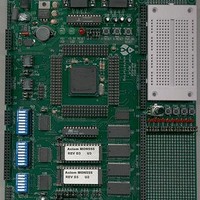
MPC555CME Freescale Semiconductor, MPC555CME Datasheet - Page 31

MPC555CME
Manufacturer Part Number
MPC555CME
Description
KIT EVALUATION FOR MPC555
Manufacturer
Freescale Semiconductor
Type
Microcontrollerr
Datasheet
1.MPC555CME.pdf
(966 pages)
Specifications of MPC555CME
Contents
Module Board, Installation Guide, Power Supply, Cable, Software and more
Processor To Be Evaluated
MPC555
Data Bus Width
32 bit
Interface Type
RS-232
For Use With/related Products
MPC555
Lead Free Status / RoHS Status
Contains lead / RoHS non-compliant
- Current page: 31 of 966
- Download datasheet (13Mb)
Number
9-1
9-2
9-3
9-4
9-5
9-6
9-7
9-8
9-9
9-10
9-11
9-12
9-13
9-14
9-15
9-16
9-17
9-18
9-19
9-20
9-21
9-22
9-23
9-24
9-25
9-26
9-27
9-28
9-29
9-30
9-31
9-32
9-33
9-34
9-35
9-36
9-37
9-38
9-39
9-40
9-41
MPC555 / MPC555
USER’S MANUAL
Figure
Input Sample Window ..................................................................................... 9-2
MPC555 / MPC556 Bus Signals ..................................................................... 9-3
Basic Transfer Protocol .................................................................................. 9-8
Basic Flow Diagram of a Single Beat Read Cycle .......................................... 9-9
Single Beat Read Cycle–Basic Timing–Zero Wait States ............................ 9-10
Single Beat Read Cycle–Basic Timing–One Wait State ............................... 9-11
Basic Flow Diagram of a Single Beat Write Cycle ........................................ 9-12
Single Beat Basic Write Cycle Timing, Zero Wait States ............................. 9-13
Single Beat Basic Write Cycle Timing, One Wait State ................................ 9-14
Single Beat 32-Bit Data
Basic Flow Diagram Of A Burst Read Cycle ................................................ 9-18
Burst-Read Cycle–32-Bit Port Size–Zero Wait State ................................... 9-19
Burst-Read Cycle–32-Bit Port Size–One Wait State .................................... 9-20
Burst-Read Cycle–32-Bit Port Size–Wait States Between Beats ................. 9-21
Burst-Read Cycle, 16-Bit Port Size .............................................................. 9-22
Basic Flow Diagram of a Burst Write Cycle .................................................. 9-23
Burst-Write Cycle, 32-Bit Port Size, Zero Wait States .................................. 9-24
Burst-Inhibit Cycle, 32-Bit Port Size (Emulated Burst) ................................. 9-25
Non-Wrap Burst with Three Beats ................................................................ 9-26
Non-Wrap Burst with One Data Beat ............................................................ 9-27
Internal Operand Representation ................................................................. 9-28
Interface To Different Port Size Devices ...................................................... 9-29
Bus Arbitration Flowchart ............................................................................. 9-31
Masters Signals Basic Connection ............................................................... 9-32
Bus Arbitration Timing Diagram .................................................................... 9-33
Internal Bus Arbitration State Machine ......................................................... 9-35
Termination Signals Protocol Basic Connection ........................................... 9-39
Termination Signals Protocol Timing Diagram ............................................. 9-40
Reservation On Local Bus ............................................................................ 9-41
Reservation On Multilevel Bus Hierarchy ..................................................... 9-42
Retry Transfer Timing–Internal Arbiter ......................................................... 9-44
Retry Transfer Timing–External Arbiter ........................................................ 9-45
Retry On Burst Cycle .................................................................................... 9-46
Basic Flow of an External Master Read Access ........................................... 9-48
Basic Flow of an External Master Write Access ........................................... 9-49
Peripheral Mode: External Master Reads
Peripheral Mode: External Master Writes to MPC555 / MPC556;
Flow of Retry of External Master Read Access ............................................ 9-53
Retry of External Master Access (Internal Arbiter) ....................................... 9-54
Instruction Show Cycle Transaction ............................................................. 9-55
Data Show Cycle Transaction ...................................................................... 9-56
Write Cycle Timing, 16 Bit-Port Size ......................................................... 9-15
from MPC555 / MPC556 — Two Wait States ........................................... 9-50
Two Wait States ........................................................................................ 9-51
Rev. 15 October 2000
LIST OF FIGURES
MOTOROLA
Number
Page
xxxi
Related parts for MPC555CME
Image
Part Number
Description
Manufacturer
Datasheet
Request
R

Part Number:
Description:
MPC555 Interrupts
Manufacturer:
Freescale Semiconductor / Motorola
Datasheet:
Part Number:
Description:
Manufacturer:
Freescale Semiconductor, Inc
Datasheet:
Part Number:
Description:
Manufacturer:
Freescale Semiconductor, Inc
Datasheet:
Part Number:
Description:
Manufacturer:
Freescale Semiconductor, Inc
Datasheet:
Part Number:
Description:
Manufacturer:
Freescale Semiconductor, Inc
Datasheet:
Part Number:
Description:
Manufacturer:
Freescale Semiconductor, Inc
Datasheet:
Part Number:
Description:
Manufacturer:
Freescale Semiconductor, Inc
Datasheet:
Part Number:
Description:
Manufacturer:
Freescale Semiconductor, Inc
Datasheet:
Part Number:
Description:
Manufacturer:
Freescale Semiconductor, Inc
Datasheet:
Part Number:
Description:
Manufacturer:
Freescale Semiconductor, Inc
Datasheet:
Part Number:
Description:
Manufacturer:
Freescale Semiconductor, Inc
Datasheet:
Part Number:
Description:
Manufacturer:
Freescale Semiconductor, Inc
Datasheet:
Part Number:
Description:
Manufacturer:
Freescale Semiconductor, Inc
Datasheet:
Part Number:
Description:
Manufacturer:
Freescale Semiconductor, Inc
Datasheet:
Part Number:
Description:
Manufacturer:
Freescale Semiconductor, Inc
Datasheet:


