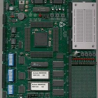
MPC555CME Freescale Semiconductor, MPC555CME Datasheet - Page 184

MPC555CME
Manufacturer Part Number
MPC555CME
Description
KIT EVALUATION FOR MPC555
Manufacturer
Freescale Semiconductor
Type
Microcontrollerr
Datasheet
1.MPC555CME.pdf
(966 pages)
Specifications of MPC555CME
Contents
Module Board, Installation Guide, Power Supply, Cable, Software and more
Processor To Be Evaluated
MPC555
Data Bus Width
32 bit
Interface Type
RS-232
For Use With/related Products
MPC555
Lead Free Status / RoHS Status
Contains lead / RoHS non-compliant
- Current page: 184 of 966
- Download datasheet (13Mb)
4.3.5 Compressed Code Address Format
MPC555
USER’S MANUAL
The format of the compressed code in memory requires special addressing. The
Decompressor module is responsible for generating compressed code addresses.
The compressed instruction stream may start on any of the 32 bits. Thus, five bits are
needed to locate such instruction inside a memory word. The instruction address in
“Decompression ON” mode consists of a 20-bit word pointer for the base address, bits
20 and 21 to show the relation between the left and right streams, and two 5-bit instruc-
tion pointers. This is known as the two-pointer address form. See
The base address contains the lowest word address of physical memory where the in-
struction resides.
The “left / right” bit, bit number 20, indicates which instruction stream side (left or right)
resides in the memory word location being pointed to by the base address. A zero “0”
for bit 20 will indicate that the left side is resident in the base address location. A one
“1” for bit 20 will indicate that the right side is resident in the base address location.
The instruction stream side not pointed to will reside in the following address location.
The “same line” bit, bit 21, reflects the relative location of the two side streams for the
instruction. If bit 21 is zero “0”, both left and right streams are located at the base ad-
dress location. In this case, bit 20 has no meaning and is a “don’t care” value of X. If
bit 21 is one “1”, then the two parts of the instruction are located in different address
word locations (one at “x” base address, the other at “x+4”).
Figure 4-8
Base Address
Compressed
Instruction
Address
/
MPC556
- Compressed Instruction
illustrates the three possible cases for bits 20 and 21.
x+4
x+8
x+c
x
Figure 4-7 Compressed Address Format
0
Rev. 15 October 2000
Word Pointer - Base Address
BURST BUFFER
:
Memory Layout
“Same Line” Bit
“Left / Right” Bit
Right Pointer Start Bit
19
1 1
22
Left
Pointer
Figure
26 27
Right
Pointer
4-7.
MOTOROLA
31
4-8
Related parts for MPC555CME
Image
Part Number
Description
Manufacturer
Datasheet
Request
R

Part Number:
Description:
MPC555 Interrupts
Manufacturer:
Freescale Semiconductor / Motorola
Datasheet:
Part Number:
Description:
Manufacturer:
Freescale Semiconductor, Inc
Datasheet:
Part Number:
Description:
Manufacturer:
Freescale Semiconductor, Inc
Datasheet:
Part Number:
Description:
Manufacturer:
Freescale Semiconductor, Inc
Datasheet:
Part Number:
Description:
Manufacturer:
Freescale Semiconductor, Inc
Datasheet:
Part Number:
Description:
Manufacturer:
Freescale Semiconductor, Inc
Datasheet:
Part Number:
Description:
Manufacturer:
Freescale Semiconductor, Inc
Datasheet:
Part Number:
Description:
Manufacturer:
Freescale Semiconductor, Inc
Datasheet:
Part Number:
Description:
Manufacturer:
Freescale Semiconductor, Inc
Datasheet:
Part Number:
Description:
Manufacturer:
Freescale Semiconductor, Inc
Datasheet:
Part Number:
Description:
Manufacturer:
Freescale Semiconductor, Inc
Datasheet:
Part Number:
Description:
Manufacturer:
Freescale Semiconductor, Inc
Datasheet:
Part Number:
Description:
Manufacturer:
Freescale Semiconductor, Inc
Datasheet:
Part Number:
Description:
Manufacturer:
Freescale Semiconductor, Inc
Datasheet:
Part Number:
Description:
Manufacturer:
Freescale Semiconductor, Inc
Datasheet:


