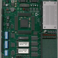
MPC555CME Freescale Semiconductor, MPC555CME Datasheet - Page 638

MPC555CME
Manufacturer Part Number
MPC555CME
Description
KIT EVALUATION FOR MPC555
Manufacturer
Freescale Semiconductor
Type
Microcontrollerr
Datasheet
1.MPC555CME.pdf
(966 pages)
Specifications of MPC555CME
Contents
Module Board, Installation Guide, Power Supply, Cable, Software and more
Processor To Be Evaluated
MPC555
Data Bus Width
32 bit
Interface Type
RS-232
For Use With/related Products
MPC555
Lead Free Status / RoHS Status
Contains lead / RoHS non-compliant
- Current page: 638 of 966
- Download datasheet (13Mb)
17.4.15 TPU3 Module Configuration Register 2
TPUMCR2 — TPU Module Configuration Register 2
MPC555
USER’S MANUAL
Bit(s)
MSB
11:13
9:10
0:6
0
0
14
15
RESET:
7
8
SOFT RST
1
0
/
ETBANK
FPSCK
MPC556
Name
DTPU
T2CF
DIV2
—
2
0
RESERVED
Reserved
Divide by 2 control. When asserted, the DIV2 bit, along with the TCR1P bit and the PSCK bit in
the TPUMCR, determines the rate of the TCR1 counter in the TPU3. If set, the TCR1 counter
increments at a rate of two IMB clocks. If negated, TCR1 increments at the rate determined by
control bits in the TCR1P and PSCK fields.
0 = TCR1 increments at rate determined by control bits in the TCR1P and PSCK fields of the
1 = Causes TCR1 counter to increment at a rate of the IMB clock divided by two
Soft reset. The TPU3 performs an internal reset when both the SOFT RST bit in the TPUMCR2
and the STOP bit in TPUMCR are set. The CPU must write zero to the SOFT RST bit to bring
the TPU3 out of reset. The SOFT RST bit must be asserted for at least nine clocks.
0 = Normal operation
1 = Puts TPU3 in reset until bit is cleared
NOTE: Do not attempt to access any other TPU3 registers when this bit is asserted. When this
bit is asserted, it is the only accessible bit in the register.
Entry table bank select. This field determines the bank where the microcoded entry table is situ-
ated. After reset, this field is 0b00. This control bit field is write once after reset. ETBANK is used
when the microcode contains entry tables not located in the default bank 0. To execute the ROM
functions on this MCU, ETBANK[1:0] must be 0b0. Refer to
NOTE: This field should not be modified by the programmer unless necessary because of cus-
tom microcode.
Filter prescaler clock. The filter prescaler clock control bit field determines the ratio between IMB
clock frequency and minimum detectable pulses. The reset value of these bits is zero, defining
the filter clock as four IMB clocks. Refer to
T2CLK pin filter control. When asserted, the T2CLK input pin is filtered with the same filter clock
that is supplied to the channels. This control bit is write once after reset.
0 = Uses fixed four-clock filter
1 = T2CLK input pin filtered with same filter clock that is supplied to the channels
Disable TPU3 pins. When the disable TPU3 control pin is asserted, pin TP15 is configured as an
input disable pin. When the TP15 pin value is zero, all TPU3 output pins are three-stated, regard-
less of the pins function. The input is not synchronized. This control bit is write once after reset.
0 = TP15 functions as normal TPU3 channel
1 = TP15 pin configured as output disable pin. When TP15 pin is low, all TPU3 output pins are
3
0
TPUMCR register
in a high-impedance state, regardless of the pin function.
Table 17-17 TPUMCR2 Bit Descriptions
4
0
5
0
TIME PROCESSOR UNIT 3
Rev. 15 October 2000
6
0
DIV2
7
0
SOFT
RST
8
0
Description
Table
9
0
ETBANK
17-19.
10
0
Table
11
0
FPSCK
17-18.
12
0
13
0
0x30 4028
0x30 4428
MOTOROLA
T2CF
14
0
DTPU
17-20
LSB
15
0
Related parts for MPC555CME
Image
Part Number
Description
Manufacturer
Datasheet
Request
R

Part Number:
Description:
MPC555 Interrupts
Manufacturer:
Freescale Semiconductor / Motorola
Datasheet:
Part Number:
Description:
Manufacturer:
Freescale Semiconductor, Inc
Datasheet:
Part Number:
Description:
Manufacturer:
Freescale Semiconductor, Inc
Datasheet:
Part Number:
Description:
Manufacturer:
Freescale Semiconductor, Inc
Datasheet:
Part Number:
Description:
Manufacturer:
Freescale Semiconductor, Inc
Datasheet:
Part Number:
Description:
Manufacturer:
Freescale Semiconductor, Inc
Datasheet:
Part Number:
Description:
Manufacturer:
Freescale Semiconductor, Inc
Datasheet:
Part Number:
Description:
Manufacturer:
Freescale Semiconductor, Inc
Datasheet:
Part Number:
Description:
Manufacturer:
Freescale Semiconductor, Inc
Datasheet:
Part Number:
Description:
Manufacturer:
Freescale Semiconductor, Inc
Datasheet:
Part Number:
Description:
Manufacturer:
Freescale Semiconductor, Inc
Datasheet:
Part Number:
Description:
Manufacturer:
Freescale Semiconductor, Inc
Datasheet:
Part Number:
Description:
Manufacturer:
Freescale Semiconductor, Inc
Datasheet:
Part Number:
Description:
Manufacturer:
Freescale Semiconductor, Inc
Datasheet:
Part Number:
Description:
Manufacturer:
Freescale Semiconductor, Inc
Datasheet:


