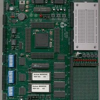
MPC555CME Freescale Semiconductor, MPC555CME Datasheet - Page 326

MPC555CME
Manufacturer Part Number
MPC555CME
Description
KIT EVALUATION FOR MPC555
Manufacturer
Freescale Semiconductor
Type
Microcontrollerr
Datasheet
1.MPC555CME.pdf
(966 pages)
Specifications of MPC555CME
Contents
Module Board, Installation Guide, Power Supply, Cable, Software and more
Processor To Be Evaluated
MPC555
Data Bus Width
32 bit
Interface Type
RS-232
For Use With/related Products
MPC555
Lead Free Status / RoHS Status
Contains lead / RoHS non-compliant
- Current page: 326 of 966
- Download datasheet (13Mb)
9.5.6 Arbitration Phase
MPC555
USER’S MANUAL
Half-word
Transfer
Word
Size
Byte
NOTE: “—” denotes a byte not required during that read cycle.
Table 9-3
MPC556 initiates an access.
NOTE: “—” denotes a byte not driven during that write cycle.
The external bus design provides for a single bus master at any one time, either the
MPC555 / MPC556 or an external device. One or more of the external devices on the
bus can have the capability of becoming bus master for the external bus. Bus arbitra-
tion may be handled either by an external central bus arbiter or by the internal on-chip
arbiter. In the latter case, the system is optimized for one external bus master besides
the MPC555 / MPC556. The arbitration configuration (external or internal) is set at sys-
tem reset.
Each bus master must have bus request (BR), bus grant (BG), and bus busy (BB) sig-
nals. The device that needs the bus asserts BR. The device then waits for the arbiter
to assert BG. In addition, the new master must look at BB to ensure that no other mas-
ter is driving the bus before it can assert BB to assume ownership of the bus. Any time
the arbiter has taken the bus grant away from the master and the master wants to ex-
Half-word
/
Transfer
MPC556
Word
Size
Byte
TSIZE
[0:1]
01
01
01
01
10
10
00
lists the patterns of the data transfer for write cycles when the MPC555 /
Table 9-2 Data Bus Requirements For Read Cycles
TSIZE[0:1]
Address
[30:31]
Table 9-3 Data Bus Contents for Write Cycles
ADDR
01
01
01
01
10
10
00
00
01
10
11
00
10
00
DATA
Address
[0:7]
OP0
OP0
OP0
[30:31]
ADDR
—
—
—
—
EXTERNAL BUS INTERFACE
00
01
10
11
00
10
00
Rev. 15 October 2000
DATA
[8:15]
OP1
OP1
OP1
—
—
—
—
32-bit Port Size
DATA
[0:7]
OP0
OP1
OP3
OP0
OP2
OP2
OP0
[16:23]
DATA
OP2
OP2
OP2
—
—
—
—
External Data Bus Pattern
DATA
[8:15]
OP1
OP3
OP1
OP3
OP1
—
—
[24:31]
DATA
OP3
OP3
OP3
—
—
—
—
[16:23]
DATA
OP2
OP2
OP2
—
—
—
—
DATA
[0:7]
16-bit Port Size
OP0
OP2
OP0
OP2
OP0
—
—
[24:31]
DATA
DATA
[8:15]
OP3
OP3
OP3
OP1
OP3
OP1
OP3
OP1
—
—
—
—
—
—
MOTOROLA
DATA
8-bit
[0:7]
Port
Size
OP0
OP1
OP2
OP3
OP0
OP2
OP0
9-30
Related parts for MPC555CME
Image
Part Number
Description
Manufacturer
Datasheet
Request
R

Part Number:
Description:
MPC555 Interrupts
Manufacturer:
Freescale Semiconductor / Motorola
Datasheet:
Part Number:
Description:
Manufacturer:
Freescale Semiconductor, Inc
Datasheet:
Part Number:
Description:
Manufacturer:
Freescale Semiconductor, Inc
Datasheet:
Part Number:
Description:
Manufacturer:
Freescale Semiconductor, Inc
Datasheet:
Part Number:
Description:
Manufacturer:
Freescale Semiconductor, Inc
Datasheet:
Part Number:
Description:
Manufacturer:
Freescale Semiconductor, Inc
Datasheet:
Part Number:
Description:
Manufacturer:
Freescale Semiconductor, Inc
Datasheet:
Part Number:
Description:
Manufacturer:
Freescale Semiconductor, Inc
Datasheet:
Part Number:
Description:
Manufacturer:
Freescale Semiconductor, Inc
Datasheet:
Part Number:
Description:
Manufacturer:
Freescale Semiconductor, Inc
Datasheet:
Part Number:
Description:
Manufacturer:
Freescale Semiconductor, Inc
Datasheet:
Part Number:
Description:
Manufacturer:
Freescale Semiconductor, Inc
Datasheet:
Part Number:
Description:
Manufacturer:
Freescale Semiconductor, Inc
Datasheet:
Part Number:
Description:
Manufacturer:
Freescale Semiconductor, Inc
Datasheet:
Part Number:
Description:
Manufacturer:
Freescale Semiconductor, Inc
Datasheet:


