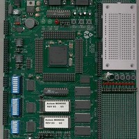
MPC555CME Freescale Semiconductor, MPC555CME Datasheet - Page 650

MPC555CME
Manufacturer Part Number
MPC555CME
Description
KIT EVALUATION FOR MPC555
Manufacturer
Freescale Semiconductor
Type
Microcontrollerr
Datasheet
1.MPC555CME.pdf
(966 pages)
Specifications of MPC555CME
Contents
Module Board, Installation Guide, Power Supply, Cable, Software and more
Processor To Be Evaluated
MPC555
Data Bus Width
32 bit
Interface Type
RS-232
For Use With/related Products
MPC555
Lead Free Status / RoHS Status
Contains lead / RoHS non-compliant
- Current page: 650 of 966
- Download datasheet (13Mb)
18.4.5 Freeze Operation
18.4.6 TPU3 Emulation Mode Operation
18.5 Multiple Input Signature Calculator (MISC)
MPC555
USER’S MANUAL
Switching to VDDSRAM occurs if VDDL drops below its specified value when the RAM
module is in stop mode.
The DPTRAM will not enter stop mode if either or both of the TP1EMM or TP2EMM
signals are asserted, indicating TPU3 emulation mode.
The FREEZE line on the IMB3 has no effect on the DPTRAM module. When the freeze
line is set, the DPTRAM module will operate in its current mode of operation. If the DP-
TRAM module is not disabled, (RAMDS = 0), it may be accessed via the IMB3. If the
DPTRAM array is being used by the TPU in emulation mode, the DPTRAM will still be
able to be accessed by the TPU microengine.
To emulate TPU3 time functions, the user stores the microinstructions required for all
time functions to be used, in the RAM array. This must be done with the DPTRAM in
its normal operating mode and accessible from the IMB3. After the time functions are
stored in the array, the user places one or both of the TPU3 units in emulation mode.
The RAM array is then controlled by the TPU3 units and disconnected from the IMB3.
To use the DPTRAM for microcode accesses, set the EMU bit in the corresponding
TPU3 module configuration register. Through the auxiliary buses, the TPU3 units can
access word instructions simultaneously at a rate of up to 40 MHz.
When the RAM array is being used by either or both of the TPU3 units, all accesses
via the IMB3 are disabled. The control registers have no effect on the RAM array. Ac-
cesses to the array are ignored, allowing an external RAM to replace the function of
the general-purpose RAM array.
The contents of the RAM are validated using a multiple input signature calculator
(MISC). MISC reads of the RAM are performed only when the MPC555 / MPC556 is
in emulation mode and the MISC is enabled (MISEN = 1 in the DPTMCR).
Refer to
eration in emulation mode.
The integrity of the RAM data is ensured through the use of a MISC. The RAM data is
read in reverse address order and a unique 32-bit signature is generated based on the
output of these reads. MISC reads are performed when one of the TPU3 modules
does not request back-to-back accesses to the RAM provided that the MISEN bit in
the DPTMCR is set.
The MISC generates the DPTRAM signature based on the following polynomial:
/
MPC556
17.3.6 Emulation Support
DUAL-PORT TPU RAM (DPTRAM)
G x ( )
Rev. 15 October 2000
=
for more information in TPU3 and DPTRAM op-
1
+ +
x
x
2
+
x
22
+
x
31
MOTOROLA
18-8
Related parts for MPC555CME
Image
Part Number
Description
Manufacturer
Datasheet
Request
R

Part Number:
Description:
MPC555 Interrupts
Manufacturer:
Freescale Semiconductor / Motorola
Datasheet:
Part Number:
Description:
Manufacturer:
Freescale Semiconductor, Inc
Datasheet:
Part Number:
Description:
Manufacturer:
Freescale Semiconductor, Inc
Datasheet:
Part Number:
Description:
Manufacturer:
Freescale Semiconductor, Inc
Datasheet:
Part Number:
Description:
Manufacturer:
Freescale Semiconductor, Inc
Datasheet:
Part Number:
Description:
Manufacturer:
Freescale Semiconductor, Inc
Datasheet:
Part Number:
Description:
Manufacturer:
Freescale Semiconductor, Inc
Datasheet:
Part Number:
Description:
Manufacturer:
Freescale Semiconductor, Inc
Datasheet:
Part Number:
Description:
Manufacturer:
Freescale Semiconductor, Inc
Datasheet:
Part Number:
Description:
Manufacturer:
Freescale Semiconductor, Inc
Datasheet:
Part Number:
Description:
Manufacturer:
Freescale Semiconductor, Inc
Datasheet:
Part Number:
Description:
Manufacturer:
Freescale Semiconductor, Inc
Datasheet:
Part Number:
Description:
Manufacturer:
Freescale Semiconductor, Inc
Datasheet:
Part Number:
Description:
Manufacturer:
Freescale Semiconductor, Inc
Datasheet:
Part Number:
Description:
Manufacturer:
Freescale Semiconductor, Inc
Datasheet:


