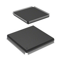
HD6417727F100CV Renesas Electronics America, HD6417727F100CV Datasheet - Page 884

HD6417727F100CV
Manufacturer Part Number
HD6417727F100CV
Description
SH3-DSP, LEAD FREE
Manufacturer
Renesas Electronics America
Series
SuperH® SH7700r
Datasheet
1.HD6417727BP100CV.pdf
(1098 pages)
Specifications of HD6417727F100CV
Core Processor
SH-3 DSP
Core Size
32-Bit
Speed
100MHz
Connectivity
FIFO, SCI, SIO, SmartCard, USB
Peripherals
DMA, LCD, POR, WDT
Number Of I /o
104
Program Memory Type
ROMless
Ram Size
32K x 8
Voltage - Supply (vcc/vdd)
1.6 V ~ 2.05 V
Data Converters
A/D 6x10b; D/A 2x8b
Oscillator Type
Internal
Operating Temperature
-20°C ~ 75°C
Package / Case
240-QFP Exposed Pad, 240-eQFP, 240-HQFP
Cpu Family
SuperH
Device Core Size
32b
Frequency (max)
100MHz
Interface Type
SCI/USB
Program Memory Size
Not Required
Total Internal Ram Size
16KB
# I/os (max)
104
Number Of Timers - General Purpose
4
Operating Supply Voltage (typ)
1.8/3.3V
Operating Supply Voltage (max)
2.05/3.6V
Operating Supply Voltage (min)
1.6/2.6V
On-chip Adc
6-chx10-bit
On-chip Dac
2-chx8-bit
Instruction Set Architecture
RISC
Operating Temp Range
-20C to 75C
Operating Temperature Classification
Commercial
Mounting
Surface Mount
Pin Count
240
Package Type
HQFP
Lead Free Status / RoHS Status
Lead free / RoHS Compliant
Eeprom Size
-
Program Memory Size
-
Lead Free Status / Rohs Status
Compliant
- Current page: 884 of 1098
- Download datasheet (7Mb)
Section 26 Pin Function Controller (PFC)
26.2
Table 26.2 summarizes the registers of the pin function controller (PFC).
Table 26.2 Pin Function Controller Registers
Name
Port A control register
Port B control register
Port C control register
Port D control register
Port E control register
Port F control register
Port G control register
Port H control register
Port J control register
Port K control register
Port L control register
SC port control register
Port M control register
Notes: These registers are located in area 1 of physical space. Therefore, when the cache is on,
Rev.6.00 Mar. 27, 2009 Page 826 of 1036
REJ09B0254-0600
either access these registers from the P2 area of logical space or else make an appropriate
setting using the MMU so that these registers are not cached.
If a low level is input at the ASEMD0 pin while the RESETP pin is asserted, ASE mode is
entered; if a high level is input, normal mode is entered. See section 31, User-Debugging
Interface (H-UDI), for more information on the H-UDI.
The initial value of the port E, F, G, and H control registers depends on the state of the
ASEMD0 pin.
* When address translation by the MMU does not apply, the address in parentheses
Register Configuration
should be used.
Abbreviation
PACR
PBCR
PCCR
PDCR
PECR
PFCR
PGCR
PHCR
PJCR
PKCR
PLCR
SCPCR
PMCR
R/W
R/W
R/W
R/W
R/W
R/W
R/W
R/W
R/W
R/W
R/W
R/W
R/W
R/W
Initial Value
H'0000
H'0000
H'AAAA
H'AAAA
H'AAAA/H'2AA8 H'04000108
H'AAAA/H'00AA H'0400010A
H'AAAA/H'A200 H'0400010C
H'AAAA/H'8AAA H'0400010E
H'0000
H'0000
H'0000
H'8008
H'AAAA
Address
H'04000100
(H'A4000100)*
H'04000102
(H'A4000102)*
H'04000104
(H'A4000104)*
H'04000106
(H'A4000106)*
(H'A4000108)*
(H'A400010A)*
(H'A400010C)*
(H'A400010E)*
H'04000110
(H'A4000110)*
H'04000112
(H'A4000112)*
H'04000114
(H'A4000114)*
H'04000116
(H'A4000116)*
H'04000118
(H'A4000118)*
Access Size
16
16
16
16
16
16
16
16
16
16
16
16
16
Related parts for HD6417727F100CV
Image
Part Number
Description
Manufacturer
Datasheet
Request
R

Part Number:
Description:
KIT STARTER FOR M16C/29
Manufacturer:
Renesas Electronics America
Datasheet:

Part Number:
Description:
KIT STARTER FOR R8C/2D
Manufacturer:
Renesas Electronics America
Datasheet:

Part Number:
Description:
R0K33062P STARTER KIT
Manufacturer:
Renesas Electronics America
Datasheet:

Part Number:
Description:
KIT STARTER FOR R8C/23 E8A
Manufacturer:
Renesas Electronics America
Datasheet:

Part Number:
Description:
KIT STARTER FOR R8C/25
Manufacturer:
Renesas Electronics America
Datasheet:

Part Number:
Description:
KIT STARTER H8S2456 SHARPE DSPLY
Manufacturer:
Renesas Electronics America
Datasheet:

Part Number:
Description:
KIT STARTER FOR R8C38C
Manufacturer:
Renesas Electronics America
Datasheet:

Part Number:
Description:
KIT STARTER FOR R8C35C
Manufacturer:
Renesas Electronics America
Datasheet:

Part Number:
Description:
KIT STARTER FOR R8CL3AC+LCD APPS
Manufacturer:
Renesas Electronics America
Datasheet:

Part Number:
Description:
KIT STARTER FOR RX610
Manufacturer:
Renesas Electronics America
Datasheet:

Part Number:
Description:
KIT STARTER FOR R32C/118
Manufacturer:
Renesas Electronics America
Datasheet:

Part Number:
Description:
KIT DEV RSK-R8C/26-29
Manufacturer:
Renesas Electronics America
Datasheet:

Part Number:
Description:
KIT STARTER FOR SH7124
Manufacturer:
Renesas Electronics America
Datasheet:

Part Number:
Description:
KIT STARTER FOR H8SX/1622
Manufacturer:
Renesas Electronics America
Datasheet:

Part Number:
Description:
KIT DEV FOR SH7203
Manufacturer:
Renesas Electronics America
Datasheet:


