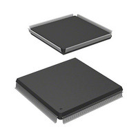
HD6417727F100CV Renesas Electronics America, HD6417727F100CV Datasheet - Page 466

HD6417727F100CV
Manufacturer Part Number
HD6417727F100CV
Description
SH3-DSP, LEAD FREE
Manufacturer
Renesas Electronics America
Series
SuperH® SH7700r
Datasheet
1.HD6417727BP100CV.pdf
(1098 pages)
Specifications of HD6417727F100CV
Core Processor
SH-3 DSP
Core Size
32-Bit
Speed
100MHz
Connectivity
FIFO, SCI, SIO, SmartCard, USB
Peripherals
DMA, LCD, POR, WDT
Number Of I /o
104
Program Memory Type
ROMless
Ram Size
32K x 8
Voltage - Supply (vcc/vdd)
1.6 V ~ 2.05 V
Data Converters
A/D 6x10b; D/A 2x8b
Oscillator Type
Internal
Operating Temperature
-20°C ~ 75°C
Package / Case
240-QFP Exposed Pad, 240-eQFP, 240-HQFP
Cpu Family
SuperH
Device Core Size
32b
Frequency (max)
100MHz
Interface Type
SCI/USB
Program Memory Size
Not Required
Total Internal Ram Size
16KB
# I/os (max)
104
Number Of Timers - General Purpose
4
Operating Supply Voltage (typ)
1.8/3.3V
Operating Supply Voltage (max)
2.05/3.6V
Operating Supply Voltage (min)
1.6/2.6V
On-chip Adc
6-chx10-bit
On-chip Dac
2-chx8-bit
Instruction Set Architecture
RISC
Operating Temp Range
-20C to 75C
Operating Temperature Classification
Commercial
Mounting
Surface Mount
Pin Count
240
Package Type
HQFP
Lead Free Status / RoHS Status
Lead free / RoHS Compliant
Eeprom Size
-
Program Memory Size
-
Lead Free Status / Rohs Status
Compliant
- Current page: 466 of 1098
- Download datasheet (7Mb)
Section 14 Direct Memory Access Controller (DMAC)
Rev.6.00 Mar. 27, 2009 Page 408 of 1036
REJ09B0254-0600
(16-byte Transfer, Transfer Source: Synchronous DRAM, Transfer Destination: Ordinary
(16-byte Transfer, Transfer Source: Ordinary Memory, Transfer Destination: Ordinary
D31 to D0
A25 to A0
Note: When DACK is output in a read cycle during transfer between external memories,
Note: When DACK is output in a read cycle during transfer between external memories,
D31 to D0
A25 to A0
DACK
Figure 14.7 Example of DMA Transfer Timing in the Direct Address Mode
Figure 14.8 Example of DMA Transfer Timing in the Direct Address Mode
CKIO
WEm
RD/WR
CSn
DACK
CKIO
RD
RAS
CAS
CSn
the output timing is the same as that of CSn.
the output timing is the same as that of CSn.
source address
Transfer
Transfer source address
Data read cycle
Data read cycle
+4
(1st cycle)
(1st cycle)
+8
Transfer destination address
Memory)
Memory)
+12
destination address
Transfer
Data write cycle
(2nd cycle)
(2nd cycle)
+4
+4
+8
+8
+12
+12
Related parts for HD6417727F100CV
Image
Part Number
Description
Manufacturer
Datasheet
Request
R

Part Number:
Description:
KIT STARTER FOR M16C/29
Manufacturer:
Renesas Electronics America
Datasheet:

Part Number:
Description:
KIT STARTER FOR R8C/2D
Manufacturer:
Renesas Electronics America
Datasheet:

Part Number:
Description:
R0K33062P STARTER KIT
Manufacturer:
Renesas Electronics America
Datasheet:

Part Number:
Description:
KIT STARTER FOR R8C/23 E8A
Manufacturer:
Renesas Electronics America
Datasheet:

Part Number:
Description:
KIT STARTER FOR R8C/25
Manufacturer:
Renesas Electronics America
Datasheet:

Part Number:
Description:
KIT STARTER H8S2456 SHARPE DSPLY
Manufacturer:
Renesas Electronics America
Datasheet:

Part Number:
Description:
KIT STARTER FOR R8C38C
Manufacturer:
Renesas Electronics America
Datasheet:

Part Number:
Description:
KIT STARTER FOR R8C35C
Manufacturer:
Renesas Electronics America
Datasheet:

Part Number:
Description:
KIT STARTER FOR R8CL3AC+LCD APPS
Manufacturer:
Renesas Electronics America
Datasheet:

Part Number:
Description:
KIT STARTER FOR RX610
Manufacturer:
Renesas Electronics America
Datasheet:

Part Number:
Description:
KIT STARTER FOR R32C/118
Manufacturer:
Renesas Electronics America
Datasheet:

Part Number:
Description:
KIT DEV RSK-R8C/26-29
Manufacturer:
Renesas Electronics America
Datasheet:

Part Number:
Description:
KIT STARTER FOR SH7124
Manufacturer:
Renesas Electronics America
Datasheet:

Part Number:
Description:
KIT STARTER FOR H8SX/1622
Manufacturer:
Renesas Electronics America
Datasheet:

Part Number:
Description:
KIT DEV FOR SH7203
Manufacturer:
Renesas Electronics America
Datasheet:


