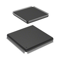
HD6417727F100CV Renesas Electronics America, HD6417727F100CV Datasheet - Page 652

HD6417727F100CV
Manufacturer Part Number
HD6417727F100CV
Description
SH3-DSP, LEAD FREE
Manufacturer
Renesas Electronics America
Series
SuperH® SH7700r
Datasheet
1.HD6417727BP100CV.pdf
(1098 pages)
Specifications of HD6417727F100CV
Core Processor
SH-3 DSP
Core Size
32-Bit
Speed
100MHz
Connectivity
FIFO, SCI, SIO, SmartCard, USB
Peripherals
DMA, LCD, POR, WDT
Number Of I /o
104
Program Memory Type
ROMless
Ram Size
32K x 8
Voltage - Supply (vcc/vdd)
1.6 V ~ 2.05 V
Data Converters
A/D 6x10b; D/A 2x8b
Oscillator Type
Internal
Operating Temperature
-20°C ~ 75°C
Package / Case
240-QFP Exposed Pad, 240-eQFP, 240-HQFP
Cpu Family
SuperH
Device Core Size
32b
Frequency (max)
100MHz
Interface Type
SCI/USB
Program Memory Size
Not Required
Total Internal Ram Size
16KB
# I/os (max)
104
Number Of Timers - General Purpose
4
Operating Supply Voltage (typ)
1.8/3.3V
Operating Supply Voltage (max)
2.05/3.6V
Operating Supply Voltage (min)
1.6/2.6V
On-chip Adc
6-chx10-bit
On-chip Dac
2-chx8-bit
Instruction Set Architecture
RISC
Operating Temp Range
-20C to 75C
Operating Temperature Classification
Commercial
Mounting
Surface Mount
Pin Count
240
Package Type
HQFP
Lead Free Status / RoHS Status
Lead free / RoHS Compliant
Eeprom Size
-
Program Memory Size
-
Lead Free Status / Rohs Status
Compliant
- Current page: 652 of 1098
- Download datasheet (7Mb)
Section 19 Serial Communication Interface with FIFO (SCIF)
In serial transmission, the SCIF operates as described below.
1. When data is written into the transmit FIFO data register 2 (SCFTDR2), the SCIF transfers the
2. When data is transferred from SCFTDR2 to SCTSR2 and transmission is started, consecutive
3. The SCIF checks the SCFTDR2 transmit data at the timing for sending the stop bit. If data is
Rev.6.00 Mar. 27, 2009 Page 594 of 1036
REJ09B0254-0600
data from SCFTDR2 to the transmit shift register 2 (SCTSR2) and starts transmitting.
Confirm that the TDFE flag in the serial status register 2 (SCSSR2) is set to 1 before writing
transmit data to SCFTDR2. The number of data bytes that can be written is (16 – transmit
trigger setting).
transmit operations are performed until there is no transmit data left in SCFTDR2. When the
number of transmit data bytes in SCFTDR2 falls below the transmit trigger number set in the
FIFO control register 2 (SCFCR2), the TDFE flag is set. If the TIE bit in the serial control
register (SCSR2) is set to 1 at this time, a transmit-FIFO-data-empty interrupt (TXI) request is
generated.
The serial transmit data is sent from the TxD2 pin in the following order.
a. Start bit: One-bit 0 is output.
b. Transmit data: 8-bit or 7-bit data is output in LSB-first order.
c. Parity bit: One parity bit (even or odd parity) is output. (A format in which a parity bit is
d. Stop bit(s): One- or two-bit 1s (stop bits) are output.
e. Mark state: 1 is output continuously until the start bit that starts the next transmission is
present, the data is transferred from SCFTDR2 to SCTSR2, the stop bit is sent, and then serial
transmission of the next frame is started.
If there is no transmit data, the TEND flag in SCSSR2 is set to 1, the stop bit is sent, and then
the line goes to the mark state in which 1 is output continuously.
Figure 19.6 shows an example of the operation for transmission.
not output can also be selected.)
sent.
Related parts for HD6417727F100CV
Image
Part Number
Description
Manufacturer
Datasheet
Request
R

Part Number:
Description:
KIT STARTER FOR M16C/29
Manufacturer:
Renesas Electronics America
Datasheet:

Part Number:
Description:
KIT STARTER FOR R8C/2D
Manufacturer:
Renesas Electronics America
Datasheet:

Part Number:
Description:
R0K33062P STARTER KIT
Manufacturer:
Renesas Electronics America
Datasheet:

Part Number:
Description:
KIT STARTER FOR R8C/23 E8A
Manufacturer:
Renesas Electronics America
Datasheet:

Part Number:
Description:
KIT STARTER FOR R8C/25
Manufacturer:
Renesas Electronics America
Datasheet:

Part Number:
Description:
KIT STARTER H8S2456 SHARPE DSPLY
Manufacturer:
Renesas Electronics America
Datasheet:

Part Number:
Description:
KIT STARTER FOR R8C38C
Manufacturer:
Renesas Electronics America
Datasheet:

Part Number:
Description:
KIT STARTER FOR R8C35C
Manufacturer:
Renesas Electronics America
Datasheet:

Part Number:
Description:
KIT STARTER FOR R8CL3AC+LCD APPS
Manufacturer:
Renesas Electronics America
Datasheet:

Part Number:
Description:
KIT STARTER FOR RX610
Manufacturer:
Renesas Electronics America
Datasheet:

Part Number:
Description:
KIT STARTER FOR R32C/118
Manufacturer:
Renesas Electronics America
Datasheet:

Part Number:
Description:
KIT DEV RSK-R8C/26-29
Manufacturer:
Renesas Electronics America
Datasheet:

Part Number:
Description:
KIT STARTER FOR SH7124
Manufacturer:
Renesas Electronics America
Datasheet:

Part Number:
Description:
KIT STARTER FOR H8SX/1622
Manufacturer:
Renesas Electronics America
Datasheet:

Part Number:
Description:
KIT DEV FOR SH7203
Manufacturer:
Renesas Electronics America
Datasheet:


