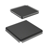
HD6417727F100CV Renesas Electronics America, HD6417727F100CV Datasheet - Page 45

HD6417727F100CV
Manufacturer Part Number
HD6417727F100CV
Description
SH3-DSP, LEAD FREE
Manufacturer
Renesas Electronics America
Series
SuperH® SH7700r
Datasheet
1.HD6417727BP100CV.pdf
(1098 pages)
Specifications of HD6417727F100CV
Core Processor
SH-3 DSP
Core Size
32-Bit
Speed
100MHz
Connectivity
FIFO, SCI, SIO, SmartCard, USB
Peripherals
DMA, LCD, POR, WDT
Number Of I /o
104
Program Memory Type
ROMless
Ram Size
32K x 8
Voltage - Supply (vcc/vdd)
1.6 V ~ 2.05 V
Data Converters
A/D 6x10b; D/A 2x8b
Oscillator Type
Internal
Operating Temperature
-20°C ~ 75°C
Package / Case
240-QFP Exposed Pad, 240-eQFP, 240-HQFP
Cpu Family
SuperH
Device Core Size
32b
Frequency (max)
100MHz
Interface Type
SCI/USB
Program Memory Size
Not Required
Total Internal Ram Size
16KB
# I/os (max)
104
Number Of Timers - General Purpose
4
Operating Supply Voltage (typ)
1.8/3.3V
Operating Supply Voltage (max)
2.05/3.6V
Operating Supply Voltage (min)
1.6/2.6V
On-chip Adc
6-chx10-bit
On-chip Dac
2-chx8-bit
Instruction Set Architecture
RISC
Operating Temp Range
-20C to 75C
Operating Temperature Classification
Commercial
Mounting
Surface Mount
Pin Count
240
Package Type
HQFP
Lead Free Status / RoHS Status
Lead free / RoHS Compliant
Eeprom Size
-
Program Memory Size
-
Lead Free Status / Rohs Status
Compliant
- Current page: 45 of 1098
- Download datasheet (7Mb)
Figure 19.2 SCPT[4]/TxD2 Pin................................................................................................. 567
Figure 19.3 SCPT[4]/RxD2 Pin................................................................................................. 568
Figure 19.4 Sample SCIF Initialization Flowchart .................................................................... 592
Figure 19.5 Sample Serial Transmission Flowchart .................................................................. 593
Figure 19.6 Example of Transmit Operation
Figure 19.7 Example of Operation Using Modem Control (CTS2)........................................... 595
Figure 19.8 Sample Serial Reception Flowchart (1).................................................................. 596
Figure 19.9 Sample Serial Reception Flowchart (2).................................................................. 597
Figure 19.10 Example of SCIF Receive Operation
Figure 19.11 Example of Operation Using Modem Control (RTS2)........................................... 599
Figure 19.12 Receive Data Sampling Timing in Asynchronous Mode ....................................... 602
Section 20 Serial IO (SIOF)
Figure 20.1 SIOF Block Diagram.............................................................................................. 606
Figure 20.2 Serial Clock Supply System ................................................................................... 630
Figure 20.3 SIOF Serial Data Synchronized Timing................................................................. 631
Figure 20.4 SIOF Transmit or Receive Timing ......................................................................... 632
Figure 20.5 Transmit or Receive Data Bit Alignment ............................................................... 634
Figure 20.6 Control Data Bit Alignment ................................................................................... 636
Figure 20.7 Control Data Interface (Slot Position).................................................................... 637
Figure 20.8 Control Data Interface (Secondary FS) .................................................................. 638
Figure 20.9 Example of Transmit Operation in Master ............................................................. 641
Figure 20.10 Example of Receive Operation in Master............................................................... 642
Figure 20.11 Example of Transmit Operation in Slave ............................................................... 643
Figure 20.12 Example of Receive Operation in Slave................................................................. 644
Figure 20.13 Transmit or Receive Timing (8 bits monaural—1) ................................................ 648
Figure 20.14 Transmit or Receive Timing (8 bits monaural—2) ................................................ 648
Figure 20.15 Transmit or Receive Timing (16 bits monaural—1) .............................................. 649
Figure 20.16 Transmit or Receive Timing (16 bits stereo—1).................................................... 649
Figure 20.17 Transmit or Receive Timing (16 bits stereo—2).................................................... 650
Figure 20.18 Transmit or Receive Timing (16 bits stereo—3).................................................... 650
Figure 20.19 Transmit or Receive Timing (16 bits monaural—2) .............................................. 651
Section 21 Analog Front End Interface (AFEIF)
Figure 21.1 Block Diagram of AFE Interface ........................................................................... 658
Figure 21.2 FIFO Interrupt Timing............................................................................................ 672
Figure 21.3 Ringing Interrupt Occurrence Timing .................................................................... 672
Figure 21.4 Interrupt Generator................................................................................................. 673
Figure 21.5 AFE Serial Interface............................................................................................... 673
(Example with 8-Bit Data, Parity, One Stop Bit) ................................................... 595
(Example with 8-Bit Data, Parity, One Stop Bit) ................................................... 599
Rev.6.00 Mar. 27, 2009 Page xliii of lvi
REJ09B0254-0600
Related parts for HD6417727F100CV
Image
Part Number
Description
Manufacturer
Datasheet
Request
R

Part Number:
Description:
KIT STARTER FOR M16C/29
Manufacturer:
Renesas Electronics America
Datasheet:

Part Number:
Description:
KIT STARTER FOR R8C/2D
Manufacturer:
Renesas Electronics America
Datasheet:

Part Number:
Description:
R0K33062P STARTER KIT
Manufacturer:
Renesas Electronics America
Datasheet:

Part Number:
Description:
KIT STARTER FOR R8C/23 E8A
Manufacturer:
Renesas Electronics America
Datasheet:

Part Number:
Description:
KIT STARTER FOR R8C/25
Manufacturer:
Renesas Electronics America
Datasheet:

Part Number:
Description:
KIT STARTER H8S2456 SHARPE DSPLY
Manufacturer:
Renesas Electronics America
Datasheet:

Part Number:
Description:
KIT STARTER FOR R8C38C
Manufacturer:
Renesas Electronics America
Datasheet:

Part Number:
Description:
KIT STARTER FOR R8C35C
Manufacturer:
Renesas Electronics America
Datasheet:

Part Number:
Description:
KIT STARTER FOR R8CL3AC+LCD APPS
Manufacturer:
Renesas Electronics America
Datasheet:

Part Number:
Description:
KIT STARTER FOR RX610
Manufacturer:
Renesas Electronics America
Datasheet:

Part Number:
Description:
KIT STARTER FOR R32C/118
Manufacturer:
Renesas Electronics America
Datasheet:

Part Number:
Description:
KIT DEV RSK-R8C/26-29
Manufacturer:
Renesas Electronics America
Datasheet:

Part Number:
Description:
KIT STARTER FOR SH7124
Manufacturer:
Renesas Electronics America
Datasheet:

Part Number:
Description:
KIT STARTER FOR H8SX/1622
Manufacturer:
Renesas Electronics America
Datasheet:

Part Number:
Description:
KIT DEV FOR SH7203
Manufacturer:
Renesas Electronics America
Datasheet:


