DS72011RB120FPV Renesas Electronics America, DS72011RB120FPV Datasheet - Page 500
DS72011RB120FPV
Manufacturer Part Number
DS72011RB120FPV
Description
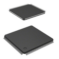
IC SH7201 MPU ROMLESS 176LQFP
Manufacturer
Renesas Electronics America
Series
SuperH® SH7200r
Datasheet
1.R0K572011S000BE.pdf
(1222 pages)
Specifications of DS72011RB120FPV
Core Size
32-Bit
Core Processor
SH-2A
Speed
120MHz
Connectivity
CAN, EBI/EMI, FIFO, I²C, SCI, Serial Sound
Peripherals
DMA, POR, PWM, WDT
Number Of I /o
104
Program Memory Type
ROMless
Ram Size
32K x 8
Voltage - Supply (vcc/vdd)
3 V ~ 3.6 V
Data Converters
A/D 8x10b; D/A 2x8b
Oscillator Type
Internal
Operating Temperature
-20°C ~ 70°C
Package / Case
176-LQFP
No. Of I/o's
109
Ram Memory Size
32KB
Cpu Speed
120MHz
Digital Ic Case Style
LQFP
Supply Voltage Range
3V To 3.6V
Operating Temperature Range
-20°C To +70°C
Embedded Interface Type
I2C, SSI
Rohs Compliant
Yes
Lead Free Status / RoHS Status
Lead free / RoHS Compliant
For Use With
R0K572011S000BE - KIT STARTER FOR SH7201HS0005KCU11H - EMULATOR E10A-USB H8S(X),SH2(A)
Eeprom Size
-
Program Memory Size
-
Lead Free Status / RoHS Status
Lead free / RoHS Compliant, Lead free / RoHS Compliant
Available stocks
Company
Part Number
Manufacturer
Quantity
Price
Company:

Part Number:
DS72011RB120FPV
Manufacturer:
Renesas Electronics America
Quantity:
10 000


Section 12 Multi-Function Timer Pulse Unit 2 (MTU2)
12.4.5
In PWM mode, PWM waveforms are output from the output pins. The output level can be selected
as 0, 1, or toggle output in response to a compare match of each TGR.
TGR registers settings can be used to output a PWM waveform in the range of 0% to 100% duty.
Designating TGR compare match as the counter clearing source enables the period to be set in that
register. All channels can be designated for PWM mode independently. Synchronous operation is
also possible.
There are two PWM modes, as described below.
1. PWM mode 1
2. PWM mode 2
Page 472 of 1190
PWM output is generated from the TIOCA and TIOCC pins by pairing TGRA with TGRB and
TGRC with TGRD. The output specified by bits IOA0 to IOA3 and IOC0 to IOC3 in TIOR is
output from the TIOCA and TIOCC pins at compare matches A and C, and the output
specified by bits IOB0 to IOB3 and IOD0 to IOD3 in TIOR is output at compare matches B
and D. The initial output value is the value set in TGRA or TGRC. If the set values of paired
TGRs are identical, the output value does not change when a compare match occurs.
In PWM mode 1, a maximum 8-phase PWM output is possible.
PWM output is generated using one TGR as the cycle register and the others as duty registers.
The output specified in TIOR is performed by means of compare matches. Upon counter
clearing by a synchronization register compare match, the output value of each pin is the initial
value set in TIOR. If the set values of the cycle and duty registers are identical, the output
value does not change when a compare match occurs.
In PWM mode 2, a maximum 8-phase PWM output is possible in combination use with
synchronous operation.
PWM Modes
R01UH0026EJ0300 Rev. 3.00
SH7201 Group
Sep 24, 2010
Related parts for DS72011RB120FPV
Image
Part Number
Description
Manufacturer
Datasheet
Request
R

Part Number:
Description:
KIT STARTER FOR M16C/29
Manufacturer:
Renesas Electronics America
Datasheet:

Part Number:
Description:
KIT STARTER FOR R8C/2D
Manufacturer:
Renesas Electronics America
Datasheet:

Part Number:
Description:
R0K33062P STARTER KIT
Manufacturer:
Renesas Electronics America
Datasheet:

Part Number:
Description:
KIT STARTER FOR R8C/23 E8A
Manufacturer:
Renesas Electronics America
Datasheet:

Part Number:
Description:
KIT STARTER FOR R8C/25
Manufacturer:
Renesas Electronics America
Datasheet:

Part Number:
Description:
KIT STARTER H8S2456 SHARPE DSPLY
Manufacturer:
Renesas Electronics America
Datasheet:

Part Number:
Description:
KIT STARTER FOR R8C38C
Manufacturer:
Renesas Electronics America
Datasheet:

Part Number:
Description:
KIT STARTER FOR R8C35C
Manufacturer:
Renesas Electronics America
Datasheet:

Part Number:
Description:
KIT STARTER FOR R8CL3AC+LCD APPS
Manufacturer:
Renesas Electronics America
Datasheet:
Part Number:
Description:
KIT STARTER FOR RX610
Manufacturer:
Renesas Electronics America
Datasheet:

Part Number:
Description:
KIT STARTER FOR R32C/118
Manufacturer:
Renesas Electronics America
Datasheet:

Part Number:
Description:
KIT DEV RSK-R8C/26-29
Manufacturer:
Renesas Electronics America
Datasheet:

Part Number:
Description:
KIT STARTER FOR SH7124
Manufacturer:
Renesas Electronics America
Datasheet:

Part Number:
Description:
KIT STARTER FOR H8SX/1622
Manufacturer:
Renesas Electronics America
Datasheet:

Part Number:
Description:
KIT DEV FOR SH7203
Manufacturer:
Renesas Electronics America
Datasheet: