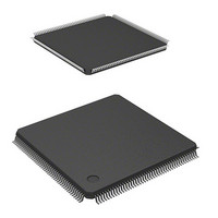
DS72011RB120FPV Renesas Electronics America, DS72011RB120FPV Datasheet - Page 238

DS72011RB120FPV
Manufacturer Part Number
DS72011RB120FPV
Description
IC SH7201 MPU ROMLESS 176LQFP
Manufacturer
Renesas Electronics America
Series
SuperH® SH7200r
Datasheet
1.R0K572011S000BE.pdf
(1222 pages)
Specifications of DS72011RB120FPV
Core Size
32-Bit
Core Processor
SH-2A
Speed
120MHz
Connectivity
CAN, EBI/EMI, FIFO, I²C, SCI, Serial Sound
Peripherals
DMA, POR, PWM, WDT
Number Of I /o
104
Program Memory Type
ROMless
Ram Size
32K x 8
Voltage - Supply (vcc/vdd)
3 V ~ 3.6 V
Data Converters
A/D 8x10b; D/A 2x8b
Oscillator Type
Internal
Operating Temperature
-20°C ~ 70°C
Package / Case
176-LQFP
No. Of I/o's
109
Ram Memory Size
32KB
Cpu Speed
120MHz
Digital Ic Case Style
LQFP
Supply Voltage Range
3V To 3.6V
Operating Temperature Range
-20°C To +70°C
Embedded Interface Type
I2C, SSI
Rohs Compliant
Yes
Lead Free Status / RoHS Status
Lead free / RoHS Compliant
For Use With
R0K572011S000BE - KIT STARTER FOR SH7201HS0005KCU11H - EMULATOR E10A-USB H8S(X),SH2(A)
Eeprom Size
-
Program Memory Size
-
Lead Free Status / RoHS Status
Lead free / RoHS Compliant, Lead free / RoHS Compliant
Available stocks
Company
Part Number
Manufacturer
Quantity
Price
Company:
Part Number:
DS72011RB120FPV
Manufacturer:
Renesas Electronics America
Quantity:
10 000
- Current page: 238 of 1222
- Download datasheet (8Mb)
Section 9 Bus State Controller (BSC)
Notes: 1. When accessing SDRAM, there is no danger of data collision on the bus due to timing.
Page 210 of 1190
Bit
19 to 16 RRCV[3:0]
15 to 0
2. Writing to the CSn recovery cycle setting register (CSnREC) must be done while CSC
Bit Name
⎯
Consequently, there is no data recovery cycle setting for SDRAM. (The value is fixed at
0 cycles.)
for the corresponding channel is disabled (EXENB = 0). Only channel 0 (CS0) can be
enabled by setting EXENB = 1. To enable channel 0, stop the DMAC and set EXENB to
1 between the reset release and data write access to CS0.
Initial
Value
0000
All 0
R/W
R/W
R
Description
Post-Read Data Recovery Cycle Setting
These bits specify the number of data recovery cycles
to be inserted after read accesses to the external bus.
If a value other than 0 is selected, data recovery cycles
are inserted in the following cases:
If a read access to the external bus is followed by a
write access to the external bus. (Data recovery cycles
are inserted even when access is performed
sequentially to the same CSC channel.)
If a read access to the external bus is followed by a
read access to a different CSC channel. (No data
recovery cycles are inserted in cases of sequential
read accesses to the same CSC channel.)
Note that if idle cycles occur between accesses to the
external bus, the number of data recovery cycles
inserted is reduced by the number of idle cycles.
0000: 0 cycle
0001: 1 cycles
1111: 15 cycles
Reserved
These bits are always read as 0. The write value
should always be 0.
:
R01UH0026EJ0300 Rev. 3.00
SH7201 Group
Sep 24, 2010
Related parts for DS72011RB120FPV
Image
Part Number
Description
Manufacturer
Datasheet
Request
R

Part Number:
Description:
KIT STARTER FOR M16C/29
Manufacturer:
Renesas Electronics America
Datasheet:

Part Number:
Description:
KIT STARTER FOR R8C/2D
Manufacturer:
Renesas Electronics America
Datasheet:

Part Number:
Description:
R0K33062P STARTER KIT
Manufacturer:
Renesas Electronics America
Datasheet:

Part Number:
Description:
KIT STARTER FOR R8C/23 E8A
Manufacturer:
Renesas Electronics America
Datasheet:

Part Number:
Description:
KIT STARTER FOR R8C/25
Manufacturer:
Renesas Electronics America
Datasheet:

Part Number:
Description:
KIT STARTER H8S2456 SHARPE DSPLY
Manufacturer:
Renesas Electronics America
Datasheet:

Part Number:
Description:
KIT STARTER FOR R8C38C
Manufacturer:
Renesas Electronics America
Datasheet:

Part Number:
Description:
KIT STARTER FOR R8C35C
Manufacturer:
Renesas Electronics America
Datasheet:

Part Number:
Description:
KIT STARTER FOR R8CL3AC+LCD APPS
Manufacturer:
Renesas Electronics America
Datasheet:

Part Number:
Description:
KIT STARTER FOR RX610
Manufacturer:
Renesas Electronics America
Datasheet:

Part Number:
Description:
KIT STARTER FOR R32C/118
Manufacturer:
Renesas Electronics America
Datasheet:

Part Number:
Description:
KIT DEV RSK-R8C/26-29
Manufacturer:
Renesas Electronics America
Datasheet:

Part Number:
Description:
KIT STARTER FOR SH7124
Manufacturer:
Renesas Electronics America
Datasheet:

Part Number:
Description:
KIT STARTER FOR H8SX/1622
Manufacturer:
Renesas Electronics America
Datasheet:

Part Number:
Description:
KIT DEV FOR SH7203
Manufacturer:
Renesas Electronics America
Datasheet:


