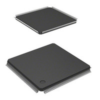
DS72011RB120FPV Renesas Electronics America, DS72011RB120FPV Datasheet - Page 269

DS72011RB120FPV
Manufacturer Part Number
DS72011RB120FPV
Description
IC SH7201 MPU ROMLESS 176LQFP
Manufacturer
Renesas Electronics America
Series
SuperH® SH7200r
Datasheet
1.R0K572011S000BE.pdf
(1222 pages)
Specifications of DS72011RB120FPV
Core Size
32-Bit
Core Processor
SH-2A
Speed
120MHz
Connectivity
CAN, EBI/EMI, FIFO, I²C, SCI, Serial Sound
Peripherals
DMA, POR, PWM, WDT
Number Of I /o
104
Program Memory Type
ROMless
Ram Size
32K x 8
Voltage - Supply (vcc/vdd)
3 V ~ 3.6 V
Data Converters
A/D 8x10b; D/A 2x8b
Oscillator Type
Internal
Operating Temperature
-20°C ~ 70°C
Package / Case
176-LQFP
No. Of I/o's
109
Ram Memory Size
32KB
Cpu Speed
120MHz
Digital Ic Case Style
LQFP
Supply Voltage Range
3V To 3.6V
Operating Temperature Range
-20°C To +70°C
Embedded Interface Type
I2C, SSI
Rohs Compliant
Yes
Lead Free Status / RoHS Status
Lead free / RoHS Compliant
For Use With
R0K572011S000BE - KIT STARTER FOR SH7201HS0005KCU11H - EMULATOR E10A-USB H8S(X),SH2(A)
Eeprom Size
-
Program Memory Size
-
Lead Free Status / RoHS Status
Lead free / RoHS Compliant, Lead free / RoHS Compliant
Available stocks
Company
Part Number
Manufacturer
Quantity
Price
Company:
Part Number:
DS72011RB120FPV
Manufacturer:
Renesas Electronics America
Quantity:
10 000
- Current page: 269 of 1222
- Download datasheet (8Mb)
SH7201 Group
1. Ts (Internal Bus Access Start)
2. Tw1 to Twn (Read Cycle Wait, Write Cycle Wait)
3. Tend (First Wait End Cycle)
R01UH0026EJ0300 Rev. 3.00
Sep 24, 2010
CKIO
A27 to A0
CSn
RD
WR
D31 to D0
This is a bus access request cycle initiated by the internal bus master and with the external bus
as the target. CSn is always high during this cycle. In the next cycle A27 to A0 and the write
data change.
For the first page access, the wait operation from internal bus access start to the wait end cycle
is the same as in normal access.
This is the final cycle in the first series of read cycle wait or write cycle wait cycles. In write
access, the second and subsequent page accesses start from the next cycle, unless a write data
output delay cycle has been specified (with a value other than 0). The RD or WR signal is
negated (high level) in the next cycle if the RD assert wait or WD assert wait setting is other
than 0. If the RD assert wait or WD assert wait setting is 0, the RD or WR signal continues to
be asserted (low level). The CSn signal is not negated and continues to be asserted (low level).
In page read access, the succeeding bus access starts without waiting for the read data sample
cycle (Trd).
Ts
CS assert wait
WR assert wait
Write data
output wait
Tw1 Tw2
Figure 9.5 Basic Bus Timing (Page Write Operation)
Write cycle wait
A0
Bus access (first time)
Twn
D0
Tend
Write data output
Write data output
Tdw1 Tdwn
delay cycle
delay cycle
Tpw1
WR assert wait
and subsequent times)
Write data
output wait
Bus access (second
Page write
cycle wait
A1
Tpwn
Tend
D1
Section 9 Bus State Controller (BSC)
Tdw1 Tdwn
Write data output
delay cycle
CS delay cycle
CS delay cycle
during write
during write
(end only)
Tn1
Tnm
Page 241 of 1190
Related parts for DS72011RB120FPV
Image
Part Number
Description
Manufacturer
Datasheet
Request
R

Part Number:
Description:
KIT STARTER FOR M16C/29
Manufacturer:
Renesas Electronics America
Datasheet:

Part Number:
Description:
KIT STARTER FOR R8C/2D
Manufacturer:
Renesas Electronics America
Datasheet:

Part Number:
Description:
R0K33062P STARTER KIT
Manufacturer:
Renesas Electronics America
Datasheet:

Part Number:
Description:
KIT STARTER FOR R8C/23 E8A
Manufacturer:
Renesas Electronics America
Datasheet:

Part Number:
Description:
KIT STARTER FOR R8C/25
Manufacturer:
Renesas Electronics America
Datasheet:

Part Number:
Description:
KIT STARTER H8S2456 SHARPE DSPLY
Manufacturer:
Renesas Electronics America
Datasheet:

Part Number:
Description:
KIT STARTER FOR R8C38C
Manufacturer:
Renesas Electronics America
Datasheet:

Part Number:
Description:
KIT STARTER FOR R8C35C
Manufacturer:
Renesas Electronics America
Datasheet:

Part Number:
Description:
KIT STARTER FOR R8CL3AC+LCD APPS
Manufacturer:
Renesas Electronics America
Datasheet:

Part Number:
Description:
KIT STARTER FOR RX610
Manufacturer:
Renesas Electronics America
Datasheet:

Part Number:
Description:
KIT STARTER FOR R32C/118
Manufacturer:
Renesas Electronics America
Datasheet:

Part Number:
Description:
KIT DEV RSK-R8C/26-29
Manufacturer:
Renesas Electronics America
Datasheet:

Part Number:
Description:
KIT STARTER FOR SH7124
Manufacturer:
Renesas Electronics America
Datasheet:

Part Number:
Description:
KIT STARTER FOR H8SX/1622
Manufacturer:
Renesas Electronics America
Datasheet:

Part Number:
Description:
KIT DEV FOR SH7203
Manufacturer:
Renesas Electronics America
Datasheet:


