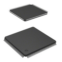
DS72011RB120FPV Renesas Electronics America, DS72011RB120FPV Datasheet - Page 412

DS72011RB120FPV
Manufacturer Part Number
DS72011RB120FPV
Description
IC SH7201 MPU ROMLESS 176LQFP
Manufacturer
Renesas Electronics America
Series
SuperH® SH7200r
Datasheet
1.R0K572011S000BE.pdf
(1222 pages)
Specifications of DS72011RB120FPV
Core Size
32-Bit
Core Processor
SH-2A
Speed
120MHz
Connectivity
CAN, EBI/EMI, FIFO, I²C, SCI, Serial Sound
Peripherals
DMA, POR, PWM, WDT
Number Of I /o
104
Program Memory Type
ROMless
Ram Size
32K x 8
Voltage - Supply (vcc/vdd)
3 V ~ 3.6 V
Data Converters
A/D 8x10b; D/A 2x8b
Oscillator Type
Internal
Operating Temperature
-20°C ~ 70°C
Package / Case
176-LQFP
No. Of I/o's
109
Ram Memory Size
32KB
Cpu Speed
120MHz
Digital Ic Case Style
LQFP
Supply Voltage Range
3V To 3.6V
Operating Temperature Range
-20°C To +70°C
Embedded Interface Type
I2C, SSI
Rohs Compliant
Yes
Lead Free Status / RoHS Status
Lead free / RoHS Compliant
For Use With
R0K572011S000BE - KIT STARTER FOR SH7201HS0005KCU11H - EMULATOR E10A-USB H8S(X),SH2(A)
Eeprom Size
-
Program Memory Size
-
Lead Free Status / RoHS Status
Lead free / RoHS Compliant, Lead free / RoHS Compliant
Available stocks
Company
Part Number
Manufacturer
Quantity
Price
Company:
Part Number:
DS72011RB120FPV
Manufacturer:
Renesas Electronics America
Quantity:
10 000
- Current page: 412 of 1222
- Download datasheet (8Mb)
Section 12 Multi-Function Timer Pulse Unit 2 (MTU2)
Table 12.10 TPSC1 and TPSC0 (Channel 5)
Note: Bits 7 to 2 are reserved in channel 5. These bits are always read as 0. The write value
12.3.2
The TMDR registers are 8-bit readable/writable registers that are used to set the operating mode of
each channel. The MTU2 has five TMDR registers, one each for channels 0 to 4. TMDR register
settings should be changed only when TCNT operation is stopped.
Page 384 of 1190
Channel
5
Bit
7
6
should always be 0.
Bit Name
—
BFE
Timer Mode Register (TMDR)
Bit 1
TPSC1
0
1
Initial value:
Initial
Value
0
0
Bit 0
TPSC0
0
1
0
1
R/W:
Bit:
—
R/W
R
R/W
R
7
0
Description
Internal clock: counts on Pφ/1
Internal clock: counts on Pφ/4
Internal clock: counts on Pφ/16
Internal clock: counts on Pφ/64
BFE
R/W
6
0
Description
Reserved
This bit is always read as 0. The write value should
always be 0.
Specifies whether TGRE_0 and TGRF_0 are to operate
in the normal way or to be used together for buffer
operation.
When TGRF is used as a buffer register, TGRF
compare match is generated.
In channels 1 to 4, this bit is reserved. It is always read
as 0 and the write value should always be 0.
0: TGRE_0 and TGRF_0 operate normally
1: TGRE_0 and TGRF_0 used together for buffer
Buffer Operation E
BFB
R/W
5
0
operation
BFA
R/W
4
0
R/W
3
0
R/W
2
0
MD[3:0]
R/W
1
0
R/W
0
0
R01UH0026EJ0300 Rev. 3.00
SH7201 Group
Sep 24, 2010
Related parts for DS72011RB120FPV
Image
Part Number
Description
Manufacturer
Datasheet
Request
R

Part Number:
Description:
KIT STARTER FOR M16C/29
Manufacturer:
Renesas Electronics America
Datasheet:

Part Number:
Description:
KIT STARTER FOR R8C/2D
Manufacturer:
Renesas Electronics America
Datasheet:

Part Number:
Description:
R0K33062P STARTER KIT
Manufacturer:
Renesas Electronics America
Datasheet:

Part Number:
Description:
KIT STARTER FOR R8C/23 E8A
Manufacturer:
Renesas Electronics America
Datasheet:

Part Number:
Description:
KIT STARTER FOR R8C/25
Manufacturer:
Renesas Electronics America
Datasheet:

Part Number:
Description:
KIT STARTER H8S2456 SHARPE DSPLY
Manufacturer:
Renesas Electronics America
Datasheet:

Part Number:
Description:
KIT STARTER FOR R8C38C
Manufacturer:
Renesas Electronics America
Datasheet:

Part Number:
Description:
KIT STARTER FOR R8C35C
Manufacturer:
Renesas Electronics America
Datasheet:

Part Number:
Description:
KIT STARTER FOR R8CL3AC+LCD APPS
Manufacturer:
Renesas Electronics America
Datasheet:

Part Number:
Description:
KIT STARTER FOR RX610
Manufacturer:
Renesas Electronics America
Datasheet:

Part Number:
Description:
KIT STARTER FOR R32C/118
Manufacturer:
Renesas Electronics America
Datasheet:

Part Number:
Description:
KIT DEV RSK-R8C/26-29
Manufacturer:
Renesas Electronics America
Datasheet:

Part Number:
Description:
KIT STARTER FOR SH7124
Manufacturer:
Renesas Electronics America
Datasheet:

Part Number:
Description:
KIT STARTER FOR H8SX/1622
Manufacturer:
Renesas Electronics America
Datasheet:

Part Number:
Description:
KIT DEV FOR SH7203
Manufacturer:
Renesas Electronics America
Datasheet:


