DS72011RB120FPV Renesas Electronics America, DS72011RB120FPV Datasheet - Page 24
DS72011RB120FPV
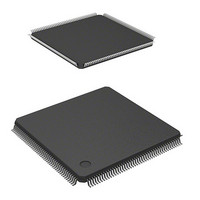
Manufacturer Part Number
DS72011RB120FPV
Description
IC SH7201 MPU ROMLESS 176LQFP
Manufacturer
Renesas Electronics America
Series
SuperH® SH7200r
Datasheet
1.R0K572011S000BE.pdf
(1222 pages)
Specifications of DS72011RB120FPV
Core Size
32-Bit
Core Processor
SH-2A
Speed
120MHz
Connectivity
CAN, EBI/EMI, FIFO, I²C, SCI, Serial Sound
Peripherals
DMA, POR, PWM, WDT
Number Of I /o
104
Program Memory Type
ROMless
Ram Size
32K x 8
Voltage - Supply (vcc/vdd)
3 V ~ 3.6 V
Data Converters
A/D 8x10b; D/A 2x8b
Oscillator Type
Internal
Operating Temperature
-20°C ~ 70°C
Package / Case
176-LQFP
No. Of I/o's
109
Ram Memory Size
32KB
Cpu Speed
120MHz
Digital Ic Case Style
LQFP
Supply Voltage Range
3V To 3.6V
Operating Temperature Range
-20°C To +70°C
Embedded Interface Type
I2C, SSI
Rohs Compliant
Yes
Lead Free Status / RoHS Status
Lead free / RoHS Compliant
For Use With
R0K572011S000BE - KIT STARTER FOR SH7201HS0005KCU11H - EMULATOR E10A-USB H8S(X),SH2(A)
Eeprom Size
-
Program Memory Size
-
Lead Free Status / RoHS Status
Lead free / RoHS Compliant, Lead free / RoHS Compliant
Available stocks
Company
Part Number
Manufacturer
Quantity
Price
Company:

Part Number:
DS72011RB120FPV
Manufacturer:
Renesas Electronics America
Quantity:
10 000


Section 20 A/D Converter (ADC) .....................................................................877
20.1
20.2
20.3
20.4
20.5
20.6
20.7
Section 21 D/A Converter (DAC) .....................................................................903
21.1
21.2
21.3
21.4
21.5
Page xxiv of xxviii
19.9.5
Features............................................................................................................................. 877
Input/Output Pins.............................................................................................................. 879
Register Configuration...................................................................................................... 880
20.3.1
20.3.2
Operation .......................................................................................................................... 886
20.4.1
20.4.2
20.4.3
20.4.4
20.4.5
20.4.6
Interrupt Sources and DMAC Transfer Request............................................................... 897
Definitions of A/D Conversion Accuracy......................................................................... 897
Usage Notes ...................................................................................................................... 899
20.7.1
20.7.2
20.7.3
20.7.4
20.7.5
20.7.6
20.7.7
Features............................................................................................................................. 903
Input/Output Pins.............................................................................................................. 904
Register Descriptions........................................................................................................ 904
21.3.1
21.3.2
Operation .......................................................................................................................... 907
Usage Notes ...................................................................................................................... 908
21.5.1
21.5.2
21.5.3
21.5.4
Interrupts........................................................................................................... 875
A/D Data Registers A to H (ADDRA to ADDRH) .......................................... 880
A/D Control/Status Register (ADCSR) ............................................................ 882
Single Mode...................................................................................................... 886
Multi Mode ....................................................................................................... 889
Scan Mode ........................................................................................................ 891
A/D Converter Activation by External Trigger, MTU2, or TMR..................... 894
Input Sampling and A/D Conversion Time ...................................................... 894
External Trigger Input Timing.......................................................................... 896
Module Standby Mode Setting ......................................................................... 899
Setting Analog Input Voltage ........................................................................... 899
Notes on Board Design ..................................................................................... 899
Processing of Analog Input Pins....................................................................... 900
Permissible Signal Source Impedance .............................................................. 901
Influences on Absolute Precision...................................................................... 902
Note on Usage in Scan Mode and Multi Mode................................................. 902
D/A Data Registers 0 and 1 (DADR0 and DADR1)......................................... 905
D/A Control Register (DACR) ......................................................................... 905
Module Standby Mode Setting ......................................................................... 908
D/A Output Hold Function in Software Standby Mode.................................... 908
D/A Conversion and D/A Output in Deep Standby Mode................................ 908
Setting Analog Input Voltage ........................................................................... 908
R01UH0026EJ0300 Rev. 3.00
Sep 24, 2010
Related parts for DS72011RB120FPV
Image
Part Number
Description
Manufacturer
Datasheet
Request
R

Part Number:
Description:
KIT STARTER FOR M16C/29
Manufacturer:
Renesas Electronics America
Datasheet:

Part Number:
Description:
KIT STARTER FOR R8C/2D
Manufacturer:
Renesas Electronics America
Datasheet:

Part Number:
Description:
R0K33062P STARTER KIT
Manufacturer:
Renesas Electronics America
Datasheet:

Part Number:
Description:
KIT STARTER FOR R8C/23 E8A
Manufacturer:
Renesas Electronics America
Datasheet:

Part Number:
Description:
KIT STARTER FOR R8C/25
Manufacturer:
Renesas Electronics America
Datasheet:

Part Number:
Description:
KIT STARTER H8S2456 SHARPE DSPLY
Manufacturer:
Renesas Electronics America
Datasheet:

Part Number:
Description:
KIT STARTER FOR R8C38C
Manufacturer:
Renesas Electronics America
Datasheet:

Part Number:
Description:
KIT STARTER FOR R8C35C
Manufacturer:
Renesas Electronics America
Datasheet:

Part Number:
Description:
KIT STARTER FOR R8CL3AC+LCD APPS
Manufacturer:
Renesas Electronics America
Datasheet:
Part Number:
Description:
KIT STARTER FOR RX610
Manufacturer:
Renesas Electronics America
Datasheet:

Part Number:
Description:
KIT STARTER FOR R32C/118
Manufacturer:
Renesas Electronics America
Datasheet:

Part Number:
Description:
KIT DEV RSK-R8C/26-29
Manufacturer:
Renesas Electronics America
Datasheet:

Part Number:
Description:
KIT STARTER FOR SH7124
Manufacturer:
Renesas Electronics America
Datasheet:

Part Number:
Description:
KIT STARTER FOR H8SX/1622
Manufacturer:
Renesas Electronics America
Datasheet:

Part Number:
Description:
KIT DEV FOR SH7203
Manufacturer:
Renesas Electronics America
Datasheet: