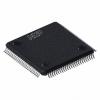
LPC1767FBD100,551 NXP Semiconductors, LPC1767FBD100,551 Datasheet - Page 582

LPC1767FBD100,551
Manufacturer Part Number
LPC1767FBD100,551
Description
IC ARM CORTEX MCU 512K 100-LQFP
Manufacturer
NXP Semiconductors
Series
LPC17xxr
Datasheets
1.LPC1767FBD100551.pdf
(2 pages)
2.LPC1767FBD100551.pdf
(840 pages)
3.LPC1767FBD100551.pdf
(65 pages)
Specifications of LPC1767FBD100,551
Core Processor
ARM® Cortex-M3™
Core Size
32-Bit
Speed
100MHz
Connectivity
Ethernet, I²C, IrDA, Microwire, SPI, SSI, UART/USART
Peripherals
Brown-out Detect/Reset, DMA, I²S, Motor Control PWM, POR, PWM, WDT
Number Of I /o
70
Program Memory Size
512KB (512K x 8)
Program Memory Type
FLASH
Ram Size
64K x 8
Voltage - Supply (vcc/vdd)
2.4 V ~ 3.6 V
Data Converters
A/D 8x12b, D/A 1x10b
Oscillator Type
Internal
Operating Temperature
-40°C ~ 85°C
Package / Case
100-LQFP
Processor Series
LPC17
Core
ARM Cortex M3
3rd Party Development Tools
MDK-ARM, RL-ARM, ULINK2, MCB1760, MCB1760U, MCB1760UME
For Use With
622-1005 - USB IN-CIRCUIT PROG ARM7 LPC2K
Lead Free Status / RoHS Status
Lead free / RoHS Compliant
Eeprom Size
-
Lead Free Status / Rohs Status
Details
Other names
568-4967
935289808551
935289808551
Available stocks
Company
Part Number
Manufacturer
Quantity
Price
Company:
Part Number:
LPC1767FBD100,551
Manufacturer:
NXP Semiconductors
Quantity:
10 000
- Current page: 582 of 840
- Download datasheet (6Mb)
30.1 Basic configuration
30.2 Features
30.3 Pin description
Table 537. D/A Pin Description
UM10360
User manual
Pin
AOUT
V
V
REFP
DDA
, V
, V
SSA
REFN
Type
Output
Reference
Power
The DAC is configured using the following registers:
Table 537
1. Power: The DAC is always connected to V
2. Clock: In the PCLKSEL0 register
3. Pins: Enable the DAC pin through the PINSEL registers. Select pin mode for port pin
4. DMA: The DAC can be connected to the GPDMA controller (see
•
•
•
•
•
•
UM10360
Chapter 30: LPC17xx Digital-to-Analog Converter (DAC)
Rev. 2 — 19 August 2010
PINSEL and PINMODE settings (see below).
with DAC through the PINMODE registers
accessing any DAC registers.
GPDMA connections, see
10-bit digital to analog converter
Resistor string architecture
Buffered output
Power-down mode
Selectable speed vs. power
Maximum update rate of 1 MHz.
Description
Analog Output. After the selected settling time after the DACR is written with a new value,
the voltage on this pin (with respect to V
Voltage References. These pins provide a voltage reference level for the ADC and DAC.
Note: V
DAC are not used.
Analog Power and Ground. These should typically be the same voltages as V
but should be isolated to minimize noise and error. Note: VDDA should be tied to VDD(3V3)
and VSSA should be tied to VSS if the ADC and DAC are not used.
gives a brief summary of each of DAC related pins.
REFP
All information provided in this document is subject to legal disclaimers.
should be tied to VDD(3V3) and V
Rev. 2 — 19 August 2010
Table
543.
(Table
SSA
) is VALUE × ((V
40), select PCLK_DAC.
DDA
(Section
REFN
. Register access is determined by
should be tied to V
8.5). This must be done before
REFP
- V
REFN
Section
)/1024) + V
© NXP B.V. 2010. All rights reserved.
SS
if the ADC and
User manual
DD
30.4.2). For
and V
REFN
582 of 840
SS
.
,
Related parts for LPC1767FBD100,551
Image
Part Number
Description
Manufacturer
Datasheet
Request
R

Part Number:
Description:
32-bit ARM Cortex-M3 microcontroller; up to 512 kB flash and 64 kB SRAM with Ethernet, USB 2.0 Host/Device/OTG, CAN
Manufacturer:
NXP [NXP Semiconductors]
Datasheet:
Part Number:
Description:
NXP Semiconductors designed the LPC2420/2460 microcontroller around a 16-bit/32-bitARM7TDMI-S CPU core with real-time debug interfaces that include both JTAG andembedded trace
Manufacturer:
NXP Semiconductors
Datasheet:

Part Number:
Description:
NXP Semiconductors designed the LPC2458 microcontroller around a 16-bit/32-bitARM7TDMI-S CPU core with real-time debug interfaces that include both JTAG andembedded trace
Manufacturer:
NXP Semiconductors
Datasheet:
Part Number:
Description:
NXP Semiconductors designed the LPC2468 microcontroller around a 16-bit/32-bitARM7TDMI-S CPU core with real-time debug interfaces that include both JTAG andembedded trace
Manufacturer:
NXP Semiconductors
Datasheet:
Part Number:
Description:
NXP Semiconductors designed the LPC2470 microcontroller, powered by theARM7TDMI-S core, to be a highly integrated microcontroller for a wide range ofapplications that require advanced communications and high quality graphic displays
Manufacturer:
NXP Semiconductors
Datasheet:
Part Number:
Description:
NXP Semiconductors designed the LPC2478 microcontroller, powered by theARM7TDMI-S core, to be a highly integrated microcontroller for a wide range ofapplications that require advanced communications and high quality graphic displays
Manufacturer:
NXP Semiconductors
Datasheet:
Part Number:
Description:
The Philips Semiconductors XA (eXtended Architecture) family of 16-bit single-chip microcontrollers is powerful enough to easily handle the requirements of high performance embedded applications, yet inexpensive enough to compete in the market for hi
Manufacturer:
NXP Semiconductors
Datasheet:
Part Number:
Description:
The XA-S3 device is a member of Philips Semiconductors? XA(eXtended Architecture) family of high performance 16-bitsingle-chip microcontrollers
Manufacturer:
NXP Semiconductors
Datasheet:

Part Number:
Description:
The NXP BlueStreak LH75401/LH75411 family consists of two low-cost 16/32-bit System-on-Chip (SoC) devices
Manufacturer:
NXP Semiconductors
Datasheet:

Part Number:
Description:
The NXP LPC3130/3131 combine an 180 MHz ARM926EJ-S CPU core, high-speed USB2
Manufacturer:
NXP Semiconductors
Datasheet:

Part Number:
Description:
The NXP LPC3141 combine a 270 MHz ARM926EJ-S CPU core, High-speed USB 2
Manufacturer:
NXP Semiconductors

Part Number:
Description:
The NXP LPC3143 combine a 270 MHz ARM926EJ-S CPU core, High-speed USB 2
Manufacturer:
NXP Semiconductors

Part Number:
Description:
The NXP LPC3152 combines an 180 MHz ARM926EJ-S CPU core, High-speed USB 2
Manufacturer:
NXP Semiconductors

Part Number:
Description:
The NXP LPC3154 combines an 180 MHz ARM926EJ-S CPU core, High-speed USB 2
Manufacturer:
NXP Semiconductors


