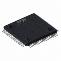
LPC1767FBD100,551 NXP Semiconductors, LPC1767FBD100,551 Datasheet - Page 415

LPC1767FBD100,551
Manufacturer Part Number
LPC1767FBD100,551
Description
IC ARM CORTEX MCU 512K 100-LQFP
Manufacturer
NXP Semiconductors
Series
LPC17xxr
Datasheets
1.LPC1767FBD100551.pdf
(2 pages)
2.LPC1767FBD100551.pdf
(840 pages)
3.LPC1767FBD100551.pdf
(65 pages)
Specifications of LPC1767FBD100,551
Core Processor
ARM® Cortex-M3™
Core Size
32-Bit
Speed
100MHz
Connectivity
Ethernet, I²C, IrDA, Microwire, SPI, SSI, UART/USART
Peripherals
Brown-out Detect/Reset, DMA, I²S, Motor Control PWM, POR, PWM, WDT
Number Of I /o
70
Program Memory Size
512KB (512K x 8)
Program Memory Type
FLASH
Ram Size
64K x 8
Voltage - Supply (vcc/vdd)
2.4 V ~ 3.6 V
Data Converters
A/D 8x12b, D/A 1x10b
Oscillator Type
Internal
Operating Temperature
-40°C ~ 85°C
Package / Case
100-LQFP
Processor Series
LPC17
Core
ARM Cortex M3
3rd Party Development Tools
MDK-ARM, RL-ARM, ULINK2, MCB1760, MCB1760U, MCB1760UME
For Use With
622-1005 - USB IN-CIRCUIT PROG ARM7 LPC2K
Lead Free Status / RoHS Status
Lead free / RoHS Compliant
Eeprom Size
-
Lead Free Status / Rohs Status
Details
Other names
568-4967
935289808551
935289808551
Available stocks
Company
Part Number
Manufacturer
Quantity
Price
Company:
Part Number:
LPC1767FBD100,551
Manufacturer:
NXP Semiconductors
Quantity:
10 000
- Current page: 415 of 840
- Download datasheet (6Mb)
NXP Semiconductors
UM10360
User manual
Fig 77. SPI frame format with CPOL=0 and CPHA=0 (a) Single and b) Continuous Transfer)
a. Single transfer with CPOL=0 and CPHA=0
b. Continuous transfer with CPOL=0 and CPHA=0
SSEL
MOSI
MISO
SCK
18.5.2.2 SPI format with CPOL=0,CPHA=0
MSB
MSB
The CPHA control bit selects the clock edge that captures data and allows it to change
state. It has the most impact on the first bit transmitted by either allowing or not allowing a
clock transition before the first data capture edge. When the CPHA phase control bit is 0,
data is captured on the first clock edge transition. If the CPHA clock phase control bit is 1,
data is captured on the second clock edge transition.
Single and continuous transmission signal sequences for SPI format with CPOL = 0,
CPHA = 0 are shown in
In this configuration, during idle periods:
If the SSP is enabled and there is valid data within the transmit FIFO, the start of
transmission is signified by the SSEL master signal being driven LOW. This causes slave
data to be enabled onto the MISO input line of the master. Master’s MOSI is enabled.
One half SCK period later, valid master data is transferred to the MOSI pin. Now that both
the master and slave data have been set, the SCK master clock pin goes HIGH after one
further half SCK period.
The data is now captured on the rising and propagated on the falling edges of the SCK
signal.
•
•
•
The CLK signal is forced LOW.
SSEL is forced HIGH.
The transmit MOSI/MISO pad is in high impedance.
SSEL
MOSI
MISO
SCK
4 to 16 bits
All information provided in this document is subject to legal disclaimers.
MSB
LSB
LSB
Rev. 2 — 19 August 2010
MSB
Figure
Q
77.
4 to 16 bits
MSB
MSB
LSB
LSB
Q
4 to 16 bits
Chapter 18: LPC17xx SSP0/1
UM10360
© NXP B.V. 2010. All rights reserved.
LSB
LSB
Q
415 of 840
Related parts for LPC1767FBD100,551
Image
Part Number
Description
Manufacturer
Datasheet
Request
R

Part Number:
Description:
32-bit ARM Cortex-M3 microcontroller; up to 512 kB flash and 64 kB SRAM with Ethernet, USB 2.0 Host/Device/OTG, CAN
Manufacturer:
NXP [NXP Semiconductors]
Datasheet:
Part Number:
Description:
NXP Semiconductors designed the LPC2420/2460 microcontroller around a 16-bit/32-bitARM7TDMI-S CPU core with real-time debug interfaces that include both JTAG andembedded trace
Manufacturer:
NXP Semiconductors
Datasheet:

Part Number:
Description:
NXP Semiconductors designed the LPC2458 microcontroller around a 16-bit/32-bitARM7TDMI-S CPU core with real-time debug interfaces that include both JTAG andembedded trace
Manufacturer:
NXP Semiconductors
Datasheet:
Part Number:
Description:
NXP Semiconductors designed the LPC2468 microcontroller around a 16-bit/32-bitARM7TDMI-S CPU core with real-time debug interfaces that include both JTAG andembedded trace
Manufacturer:
NXP Semiconductors
Datasheet:
Part Number:
Description:
NXP Semiconductors designed the LPC2470 microcontroller, powered by theARM7TDMI-S core, to be a highly integrated microcontroller for a wide range ofapplications that require advanced communications and high quality graphic displays
Manufacturer:
NXP Semiconductors
Datasheet:
Part Number:
Description:
NXP Semiconductors designed the LPC2478 microcontroller, powered by theARM7TDMI-S core, to be a highly integrated microcontroller for a wide range ofapplications that require advanced communications and high quality graphic displays
Manufacturer:
NXP Semiconductors
Datasheet:
Part Number:
Description:
The Philips Semiconductors XA (eXtended Architecture) family of 16-bit single-chip microcontrollers is powerful enough to easily handle the requirements of high performance embedded applications, yet inexpensive enough to compete in the market for hi
Manufacturer:
NXP Semiconductors
Datasheet:
Part Number:
Description:
The XA-S3 device is a member of Philips Semiconductors? XA(eXtended Architecture) family of high performance 16-bitsingle-chip microcontrollers
Manufacturer:
NXP Semiconductors
Datasheet:

Part Number:
Description:
The NXP BlueStreak LH75401/LH75411 family consists of two low-cost 16/32-bit System-on-Chip (SoC) devices
Manufacturer:
NXP Semiconductors
Datasheet:

Part Number:
Description:
The NXP LPC3130/3131 combine an 180 MHz ARM926EJ-S CPU core, high-speed USB2
Manufacturer:
NXP Semiconductors
Datasheet:

Part Number:
Description:
The NXP LPC3141 combine a 270 MHz ARM926EJ-S CPU core, High-speed USB 2
Manufacturer:
NXP Semiconductors

Part Number:
Description:
The NXP LPC3143 combine a 270 MHz ARM926EJ-S CPU core, High-speed USB 2
Manufacturer:
NXP Semiconductors

Part Number:
Description:
The NXP LPC3152 combines an 180 MHz ARM926EJ-S CPU core, High-speed USB 2
Manufacturer:
NXP Semiconductors

Part Number:
Description:
The NXP LPC3154 combines an 180 MHz ARM926EJ-S CPU core, High-speed USB 2
Manufacturer:
NXP Semiconductors


