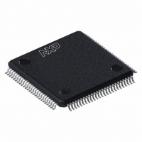
LPC1767FBD100,551 NXP Semiconductors, LPC1767FBD100,551 Datasheet - Page 156

LPC1767FBD100,551
Manufacturer Part Number
LPC1767FBD100,551
Description
IC ARM CORTEX MCU 512K 100-LQFP
Manufacturer
NXP Semiconductors
Series
LPC17xxr
Datasheets
1.LPC1767FBD100551.pdf
(2 pages)
2.LPC1767FBD100551.pdf
(840 pages)
3.LPC1767FBD100551.pdf
(65 pages)
Specifications of LPC1767FBD100,551
Core Processor
ARM® Cortex-M3™
Core Size
32-Bit
Speed
100MHz
Connectivity
Ethernet, I²C, IrDA, Microwire, SPI, SSI, UART/USART
Peripherals
Brown-out Detect/Reset, DMA, I²S, Motor Control PWM, POR, PWM, WDT
Number Of I /o
70
Program Memory Size
512KB (512K x 8)
Program Memory Type
FLASH
Ram Size
64K x 8
Voltage - Supply (vcc/vdd)
2.4 V ~ 3.6 V
Data Converters
A/D 8x12b, D/A 1x10b
Oscillator Type
Internal
Operating Temperature
-40°C ~ 85°C
Package / Case
100-LQFP
Processor Series
LPC17
Core
ARM Cortex M3
3rd Party Development Tools
MDK-ARM, RL-ARM, ULINK2, MCB1760, MCB1760U, MCB1760UME
For Use With
622-1005 - USB IN-CIRCUIT PROG ARM7 LPC2K
Lead Free Status / RoHS Status
Lead free / RoHS Compliant
Eeprom Size
-
Lead Free Status / Rohs Status
Details
Other names
568-4967
935289808551
935289808551
Available stocks
Company
Part Number
Manufacturer
Quantity
Price
Company:
Part Number:
LPC1767FBD100,551
Manufacturer:
NXP Semiconductors
Quantity:
10 000
- Current page: 156 of 840
- Download datasheet (6Mb)
NXP Semiconductors
UM10360
User manual
10.11.13 MII Mgmt Read Data Register (MRDD - 0x5000 0030)
10.11.14 MII Mgmt Indicators Register (MIND - 0x5000 0034)
Table 142. MII Mgmt Write Data register (MWTD - address 0x5000 002C) bit description
The MII Mgmt Read Data register (MRDD) is a read-only register with an address of
0x5000 0030. The bit definition of this register is shown in
Table 143. MII Mgmt Read Data register (MRDD - address 0x5000 0030) bit description
The MII Mgmt Indicators register (MIND) is a read-only register with an address of
0x5000 0034. The bit definition of this register is shown in
Table 144. MII Mgmt Indicators register (MIND - address 0x5000 0034) bit description
Here are two examples to access PHY via the MII Management Controller.
For PHY Write if scan is not used:
For PHY Read if scan is not used:
Bit
15:0
31:16 -
Bit
15:0
31:16 -
Bit
0
1
2
3
31:4
1. Write 0 to MCMD
2. Write PHY address and register address to MADR
3. Write data to MWTD
4. Wait for busy bit to be cleared in MIND
1. Write 1 to MCMD
2. Write PHY address and register address to MADR
Symbol
WRITE
DATA
Symbol
READ
DATA
Symbol
BUSY
SCANNING When ’1’ is returned - indicates a scan operation (continuous MII
NOT VALID
MII Link Fail When ’1’ is returned - indicates that an MII Mgmt link fail has
-
All information provided in this document is subject to legal disclaimers.
Function
Following an MII Mgmt Read Cycle, the 16-bit data can be read from
this location.
Unused
Function
When written, an MII Mgmt write cycle is performed using the 16-bit
data and the pre-configured PHY and Register addresses from the
MII Mgmt Address register (MADR).
Unused
Function
When ’1’ is returned - indicates MII Mgmt is currently performing an
MII Mgmt Read or Write cycle.
Mgmt Read cycles) is in progress.
When ’1’ is returned - indicates MII Mgmt Read cycle has not
completed and the Read Data is not yet valid.
occurred.
Unused
Rev. 2 — 19 August 2010
Chapter 10: LPC17xx Ethernet
Table
Table
143.
144.
UM10360
© NXP B.V. 2010. All rights reserved.
156 of 840
Reset
value
0x0
0x0
Reset
value
0x0
0x0
Reset
value
0
0
0
0
0x0
Related parts for LPC1767FBD100,551
Image
Part Number
Description
Manufacturer
Datasheet
Request
R

Part Number:
Description:
32-bit ARM Cortex-M3 microcontroller; up to 512 kB flash and 64 kB SRAM with Ethernet, USB 2.0 Host/Device/OTG, CAN
Manufacturer:
NXP [NXP Semiconductors]
Datasheet:
Part Number:
Description:
NXP Semiconductors designed the LPC2420/2460 microcontroller around a 16-bit/32-bitARM7TDMI-S CPU core with real-time debug interfaces that include both JTAG andembedded trace
Manufacturer:
NXP Semiconductors
Datasheet:

Part Number:
Description:
NXP Semiconductors designed the LPC2458 microcontroller around a 16-bit/32-bitARM7TDMI-S CPU core with real-time debug interfaces that include both JTAG andembedded trace
Manufacturer:
NXP Semiconductors
Datasheet:
Part Number:
Description:
NXP Semiconductors designed the LPC2468 microcontroller around a 16-bit/32-bitARM7TDMI-S CPU core with real-time debug interfaces that include both JTAG andembedded trace
Manufacturer:
NXP Semiconductors
Datasheet:
Part Number:
Description:
NXP Semiconductors designed the LPC2470 microcontroller, powered by theARM7TDMI-S core, to be a highly integrated microcontroller for a wide range ofapplications that require advanced communications and high quality graphic displays
Manufacturer:
NXP Semiconductors
Datasheet:
Part Number:
Description:
NXP Semiconductors designed the LPC2478 microcontroller, powered by theARM7TDMI-S core, to be a highly integrated microcontroller for a wide range ofapplications that require advanced communications and high quality graphic displays
Manufacturer:
NXP Semiconductors
Datasheet:
Part Number:
Description:
The Philips Semiconductors XA (eXtended Architecture) family of 16-bit single-chip microcontrollers is powerful enough to easily handle the requirements of high performance embedded applications, yet inexpensive enough to compete in the market for hi
Manufacturer:
NXP Semiconductors
Datasheet:
Part Number:
Description:
The XA-S3 device is a member of Philips Semiconductors? XA(eXtended Architecture) family of high performance 16-bitsingle-chip microcontrollers
Manufacturer:
NXP Semiconductors
Datasheet:

Part Number:
Description:
The NXP BlueStreak LH75401/LH75411 family consists of two low-cost 16/32-bit System-on-Chip (SoC) devices
Manufacturer:
NXP Semiconductors
Datasheet:

Part Number:
Description:
The NXP LPC3130/3131 combine an 180 MHz ARM926EJ-S CPU core, high-speed USB2
Manufacturer:
NXP Semiconductors
Datasheet:

Part Number:
Description:
The NXP LPC3141 combine a 270 MHz ARM926EJ-S CPU core, High-speed USB 2
Manufacturer:
NXP Semiconductors

Part Number:
Description:
The NXP LPC3143 combine a 270 MHz ARM926EJ-S CPU core, High-speed USB 2
Manufacturer:
NXP Semiconductors

Part Number:
Description:
The NXP LPC3152 combines an 180 MHz ARM926EJ-S CPU core, High-speed USB 2
Manufacturer:
NXP Semiconductors

Part Number:
Description:
The NXP LPC3154 combines an 180 MHz ARM926EJ-S CPU core, High-speed USB 2
Manufacturer:
NXP Semiconductors


