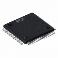
LPC1767FBD100,551 NXP Semiconductors, LPC1767FBD100,551 Datasheet - Page 574

LPC1767FBD100,551
Manufacturer Part Number
LPC1767FBD100,551
Description
IC ARM CORTEX MCU 512K 100-LQFP
Manufacturer
NXP Semiconductors
Series
LPC17xxr
Datasheets
1.LPC1767FBD100551.pdf
(2 pages)
2.LPC1767FBD100551.pdf
(840 pages)
3.LPC1767FBD100551.pdf
(65 pages)
Specifications of LPC1767FBD100,551
Core Processor
ARM® Cortex-M3™
Core Size
32-Bit
Speed
100MHz
Connectivity
Ethernet, I²C, IrDA, Microwire, SPI, SSI, UART/USART
Peripherals
Brown-out Detect/Reset, DMA, I²S, Motor Control PWM, POR, PWM, WDT
Number Of I /o
70
Program Memory Size
512KB (512K x 8)
Program Memory Type
FLASH
Ram Size
64K x 8
Voltage - Supply (vcc/vdd)
2.4 V ~ 3.6 V
Data Converters
A/D 8x12b, D/A 1x10b
Oscillator Type
Internal
Operating Temperature
-40°C ~ 85°C
Package / Case
100-LQFP
Processor Series
LPC17
Core
ARM Cortex M3
3rd Party Development Tools
MDK-ARM, RL-ARM, ULINK2, MCB1760, MCB1760U, MCB1760UME
For Use With
622-1005 - USB IN-CIRCUIT PROG ARM7 LPC2K
Lead Free Status / RoHS Status
Lead free / RoHS Compliant
Eeprom Size
-
Lead Free Status / Rohs Status
Details
Other names
568-4967
935289808551
935289808551
Available stocks
Company
Part Number
Manufacturer
Quantity
Price
Company:
Part Number:
LPC1767FBD100,551
Manufacturer:
NXP Semiconductors
Quantity:
10 000
- Current page: 574 of 840
- Download datasheet (6Mb)
29.1 Basic configuration
29.2 Features
29.3 Description
UM10360
User manual
The ADC is configured using the following registers:
Basic clocking for the A/D converters is provided by the APB clock. A programmable
divider is included in each converter to scale this clock to the clock (maximum 13 MHz)
needed by the successive approximation process. A fully accurate conversion requires 65
of these clocks.
1. Power: In the PCONP register
2. Clock: In the PCLKSEL0 register
3. Pins: Enable ADC0 pins through PINSEL registers. Select the pin modes for the port
4. Interrupts: To enable interrupts in the ADC, see
5. DMA: See
•
•
•
•
•
•
•
UM10360
Chapter 29: LPC17xx Analog-to-Digital Converter (ADC)
Rev. 2 — 19 August 2010
Remark: On reset, the ADC is disabled. To enable the ADC, first set the PCADC bit,
and then enable the ADC in the AD0CR register (bit PDN
ADC, first clear the PDN bit, and then clear the PCADC bit.
the ADC, see bits CLKDIV in
pins with ADC0 functions through the PINMODE registers
the NVIC using the appropriate Interrupt Set Enable register. Disable the ADC
interrupt in the NVIC using the appropriate Interrupt Set Enable register.
12-bit successive approximation analog to digital converter.
Input multiplexing among 8 pins.
Power-down mode.
Measurement range V
12-bit conversion rate of 200 kHz.
Burst conversion mode for single or multiple inputs.
Optional conversion on transition on input pin or Timer Match signal.
Section
All information provided in this document is subject to legal disclaimers.
Rev. 2 — 19 August 2010
29.6.4. For GPDMA system connections, see
REFN
to V
Table
(Table
REFP
(Table
531.
(typically 3 V; not to exceed V
46), set the PCADC bit.
40), select PCLK_ADC. To scale the clock for
Table
535. Interrupts are enabled in
Table
(Section
531). To disable the
Table
DDA
© NXP B.V. 2010. All rights reserved.
8.5).
User manual
voltage level).
543.
574 of 840
Related parts for LPC1767FBD100,551
Image
Part Number
Description
Manufacturer
Datasheet
Request
R

Part Number:
Description:
32-bit ARM Cortex-M3 microcontroller; up to 512 kB flash and 64 kB SRAM with Ethernet, USB 2.0 Host/Device/OTG, CAN
Manufacturer:
NXP [NXP Semiconductors]
Datasheet:
Part Number:
Description:
NXP Semiconductors designed the LPC2420/2460 microcontroller around a 16-bit/32-bitARM7TDMI-S CPU core with real-time debug interfaces that include both JTAG andembedded trace
Manufacturer:
NXP Semiconductors
Datasheet:

Part Number:
Description:
NXP Semiconductors designed the LPC2458 microcontroller around a 16-bit/32-bitARM7TDMI-S CPU core with real-time debug interfaces that include both JTAG andembedded trace
Manufacturer:
NXP Semiconductors
Datasheet:
Part Number:
Description:
NXP Semiconductors designed the LPC2468 microcontroller around a 16-bit/32-bitARM7TDMI-S CPU core with real-time debug interfaces that include both JTAG andembedded trace
Manufacturer:
NXP Semiconductors
Datasheet:
Part Number:
Description:
NXP Semiconductors designed the LPC2470 microcontroller, powered by theARM7TDMI-S core, to be a highly integrated microcontroller for a wide range ofapplications that require advanced communications and high quality graphic displays
Manufacturer:
NXP Semiconductors
Datasheet:
Part Number:
Description:
NXP Semiconductors designed the LPC2478 microcontroller, powered by theARM7TDMI-S core, to be a highly integrated microcontroller for a wide range ofapplications that require advanced communications and high quality graphic displays
Manufacturer:
NXP Semiconductors
Datasheet:
Part Number:
Description:
The Philips Semiconductors XA (eXtended Architecture) family of 16-bit single-chip microcontrollers is powerful enough to easily handle the requirements of high performance embedded applications, yet inexpensive enough to compete in the market for hi
Manufacturer:
NXP Semiconductors
Datasheet:
Part Number:
Description:
The XA-S3 device is a member of Philips Semiconductors? XA(eXtended Architecture) family of high performance 16-bitsingle-chip microcontrollers
Manufacturer:
NXP Semiconductors
Datasheet:

Part Number:
Description:
The NXP BlueStreak LH75401/LH75411 family consists of two low-cost 16/32-bit System-on-Chip (SoC) devices
Manufacturer:
NXP Semiconductors
Datasheet:

Part Number:
Description:
The NXP LPC3130/3131 combine an 180 MHz ARM926EJ-S CPU core, high-speed USB2
Manufacturer:
NXP Semiconductors
Datasheet:

Part Number:
Description:
The NXP LPC3141 combine a 270 MHz ARM926EJ-S CPU core, High-speed USB 2
Manufacturer:
NXP Semiconductors

Part Number:
Description:
The NXP LPC3143 combine a 270 MHz ARM926EJ-S CPU core, High-speed USB 2
Manufacturer:
NXP Semiconductors

Part Number:
Description:
The NXP LPC3152 combines an 180 MHz ARM926EJ-S CPU core, High-speed USB 2
Manufacturer:
NXP Semiconductors

Part Number:
Description:
The NXP LPC3154 combines an 180 MHz ARM926EJ-S CPU core, High-speed USB 2
Manufacturer:
NXP Semiconductors


