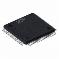
LPC1767FBD100,551 NXP Semiconductors, LPC1767FBD100,551 Datasheet - Page 318

LPC1767FBD100,551
Manufacturer Part Number
LPC1767FBD100,551
Description
IC ARM CORTEX MCU 512K 100-LQFP
Manufacturer
NXP Semiconductors
Series
LPC17xxr
Datasheets
1.LPC1767FBD100551.pdf
(2 pages)
2.LPC1767FBD100551.pdf
(840 pages)
3.LPC1767FBD100551.pdf
(65 pages)
Specifications of LPC1767FBD100,551
Core Processor
ARM® Cortex-M3™
Core Size
32-Bit
Speed
100MHz
Connectivity
Ethernet, I²C, IrDA, Microwire, SPI, SSI, UART/USART
Peripherals
Brown-out Detect/Reset, DMA, I²S, Motor Control PWM, POR, PWM, WDT
Number Of I /o
70
Program Memory Size
512KB (512K x 8)
Program Memory Type
FLASH
Ram Size
64K x 8
Voltage - Supply (vcc/vdd)
2.4 V ~ 3.6 V
Data Converters
A/D 8x12b, D/A 1x10b
Oscillator Type
Internal
Operating Temperature
-40°C ~ 85°C
Package / Case
100-LQFP
Processor Series
LPC17
Core
ARM Cortex M3
3rd Party Development Tools
MDK-ARM, RL-ARM, ULINK2, MCB1760, MCB1760U, MCB1760UME
For Use With
622-1005 - USB IN-CIRCUIT PROG ARM7 LPC2K
Lead Free Status / RoHS Status
Lead free / RoHS Compliant
Eeprom Size
-
Lead Free Status / Rohs Status
Details
Other names
568-4967
935289808551
935289808551
Available stocks
Company
Part Number
Manufacturer
Quantity
Price
Company:
Part Number:
LPC1767FBD100,551
Manufacturer:
NXP Semiconductors
Quantity:
10 000
- Current page: 318 of 840
- Download datasheet (6Mb)
15.1 Basic configuration
15.2 Features
UM10360
User manual
The UART1 peripheral is configured using the following registers:
1. Power: In the PCONP register
2. Peripheral clock: In the PCLKSEL0 register
3. Baud rate: In register U1LCR
4. UART FIFO: Use bit FIFO enable (bit 0) in register U0FCR
5. Pins: Select UART pins through PINSEL registers and pin modes through the
6. Interrupts: To enable UART interrupts set bit DLAB =0 in register U1LCR
7. DMA: UART1 transmit and receive functions can operated with the GPDMA controller
•
•
•
•
•
•
•
•
•
•
•
UM10360
Chapter 15: LPC17xx UART1
Rev. 2 — 19 August 2010
Remark: On reset, UART1 is enabled (PCUART1 = 1).
registers DLL
needed, set the fractional baud rate in the fractional divider register
FIFO.
PINMODE registers
Remark: UART receive pins should not have pull-down resistors enabled.
This enables access to U1IER
the appropriate Interrupt Set Enable register.
(see
Full modem control handshaking available
Data sizes of 5, 6, 7, and 8 bits.
Parity generation and checking: odd, even mark, space or none.
One or two stop bits.
16 byte Receive and Transmit FIFOs.
Built-in baud rate generator, including a fractional rate divider for great versatility.
Supports DMA for both transmit and receive.
Auto-baud capability
Break generation and detection.
Multiprocessor addressing mode.
RS-485 support.
Table
543).
All information provided in this document is subject to legal disclaimers.
(Table
Rev. 2 — 19 August 2010
(Section
292) and DLM
8.5).
(Table
(Table
(Table
(Table
298), set bit DLAB =1. This enables access to
46), set bits PCUART1.
294). Interrupts are enabled in the NVIC using
293) for setting the baud rate. Also, if
(Table
40), select PCLK_UART1.
(Table
297) to enable
© NXP B.V. 2010. All rights reserved.
(Table
User manual
(Table
305).
318 of 840
298).
Related parts for LPC1767FBD100,551
Image
Part Number
Description
Manufacturer
Datasheet
Request
R

Part Number:
Description:
32-bit ARM Cortex-M3 microcontroller; up to 512 kB flash and 64 kB SRAM with Ethernet, USB 2.0 Host/Device/OTG, CAN
Manufacturer:
NXP [NXP Semiconductors]
Datasheet:
Part Number:
Description:
NXP Semiconductors designed the LPC2420/2460 microcontroller around a 16-bit/32-bitARM7TDMI-S CPU core with real-time debug interfaces that include both JTAG andembedded trace
Manufacturer:
NXP Semiconductors
Datasheet:

Part Number:
Description:
NXP Semiconductors designed the LPC2458 microcontroller around a 16-bit/32-bitARM7TDMI-S CPU core with real-time debug interfaces that include both JTAG andembedded trace
Manufacturer:
NXP Semiconductors
Datasheet:
Part Number:
Description:
NXP Semiconductors designed the LPC2468 microcontroller around a 16-bit/32-bitARM7TDMI-S CPU core with real-time debug interfaces that include both JTAG andembedded trace
Manufacturer:
NXP Semiconductors
Datasheet:
Part Number:
Description:
NXP Semiconductors designed the LPC2470 microcontroller, powered by theARM7TDMI-S core, to be a highly integrated microcontroller for a wide range ofapplications that require advanced communications and high quality graphic displays
Manufacturer:
NXP Semiconductors
Datasheet:
Part Number:
Description:
NXP Semiconductors designed the LPC2478 microcontroller, powered by theARM7TDMI-S core, to be a highly integrated microcontroller for a wide range ofapplications that require advanced communications and high quality graphic displays
Manufacturer:
NXP Semiconductors
Datasheet:
Part Number:
Description:
The Philips Semiconductors XA (eXtended Architecture) family of 16-bit single-chip microcontrollers is powerful enough to easily handle the requirements of high performance embedded applications, yet inexpensive enough to compete in the market for hi
Manufacturer:
NXP Semiconductors
Datasheet:
Part Number:
Description:
The XA-S3 device is a member of Philips Semiconductors? XA(eXtended Architecture) family of high performance 16-bitsingle-chip microcontrollers
Manufacturer:
NXP Semiconductors
Datasheet:

Part Number:
Description:
The NXP BlueStreak LH75401/LH75411 family consists of two low-cost 16/32-bit System-on-Chip (SoC) devices
Manufacturer:
NXP Semiconductors
Datasheet:

Part Number:
Description:
The NXP LPC3130/3131 combine an 180 MHz ARM926EJ-S CPU core, high-speed USB2
Manufacturer:
NXP Semiconductors
Datasheet:

Part Number:
Description:
The NXP LPC3141 combine a 270 MHz ARM926EJ-S CPU core, High-speed USB 2
Manufacturer:
NXP Semiconductors

Part Number:
Description:
The NXP LPC3143 combine a 270 MHz ARM926EJ-S CPU core, High-speed USB 2
Manufacturer:
NXP Semiconductors

Part Number:
Description:
The NXP LPC3152 combines an 180 MHz ARM926EJ-S CPU core, High-speed USB 2
Manufacturer:
NXP Semiconductors

Part Number:
Description:
The NXP LPC3154 combines an 180 MHz ARM926EJ-S CPU core, High-speed USB 2
Manufacturer:
NXP Semiconductors


