MC56F8257MLH Freescale Semiconductor, MC56F8257MLH Datasheet - Page 88
MC56F8257MLH
Manufacturer Part Number
MC56F8257MLH
Description
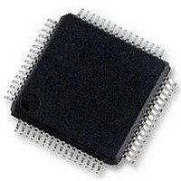
DSC 64K FLASH 60MHZ 64-LQFP
Manufacturer
Freescale Semiconductor
Series
56F8xxxr
Datasheets
1.TWR-56F8257.pdf
(88 pages)
2.MC56F8245VLD.pdf
(14 pages)
3.MC56F8245VLD.pdf
(2 pages)
4.MC56F8245VLD.pdf
(629 pages)
Specifications of MC56F8257MLH
Core Processor
56800E
Core Size
16-Bit
Speed
60MHz
Connectivity
CAN, I²C, LIN, SCI, SPI
Peripherals
LVD, POR, PWM, WDT
Number Of I /o
54
Program Memory Size
64KB (32K x 16)
Program Memory Type
FLASH
Ram Size
4K x 16
Voltage - Supply (vcc/vdd)
3 V ~ 3.6 V
Data Converters
A/D 16x12b, D/A 1x12b
Oscillator Type
Internal
Operating Temperature
-40°C ~ 105°C
Package / Case
64-LQFP
Product
DSCs
Processor Series
56800E
Core
56800E
Device Million Instructions Per Second
60 MIPs
Maximum Clock Frequency
60 MHz
Number Of Programmable I/os
54
Data Ram Size
8 KB
Operating Supply Voltage
3.3 V
Maximum Operating Temperature
+ 105 C
Mounting Style
SMD/SMT
Minimum Operating Temperature
- 40 C
On-chip Adc
12 bit, 8 Channel
Lead Free Status / RoHS Status
Lead free / RoHS Compliant
Eeprom Size
-
Lead Free Status / Rohs Status
Details
Available stocks
Company
Part Number
Manufacturer
Quantity
Price
Company:

Part Number:
MC56F8257MLH
Manufacturer:
MOTOLOLA
Quantity:
560
Company:
Part Number:
MC56F8257MLH
Manufacturer:
Freescale Semiconductor
Quantity:
10 000


Functional Description
2.4.3 ADC Data Processing
The result of an ADC conversion process is normally sent to an adder for offset
correction, as the following figure shows. The adder subtracts the ADC_OFFST register
value from each sample, and the resultant value is stored in the result register (RSLT).
The raw ADC value and the RSLT values are checked for limit violations and zero-
crossing, as shown. Appropriate interrupts are asserted, if enabled.
The result value sign is determined from the ADC unsigned result minus the respective
offset register value. If the offset register is programmed with a value of zero, the result
register value is unsigned and equals the cyclic converter unsigned result. The range of
the result (RSLT) is 0000H–7FF8H, assuming that the offset register (OFFST) is cleared
to all zeros. This is equal to the raw value of the ADC core.
The processor can write the result registers used for the results of a scan when the STOP
bit for that scan is asserted. This write operation is treated as if it comes from the ADC
analog core, so the limit checking, zero crossing, and the offset registers function as if in
normal mode. For example, if the STOP bit is set to one and the processor writes to
RSLT5, the data written to the RSLT5 is multiplexed to the ADC digital logic inputs,
processed, and stored into RSLT5 as if the analog core had provided the data. This test
data must be justified, as illustrated by the RSLT register definition and does not include
the sign bit.
88
Figure 2-71. Typical Connections for Differential Measurements
V
REFH
Potential
MC56F825x/4x Reference Manual, Rev. 2, 10/2010
- -
Differential buffer centers about mid-point.
Center tap held at (V
+
V
REF
/2
AN+
AN–
REFH
Preliminary
+ V
AN+
AN–
Note: Normally, VREFLO is set to VSSA = 0 V.
REFLO
)/2.
Freescale Semiconductor
Related parts for MC56F8257MLH
Image
Part Number
Description
Manufacturer
Datasheet
Request
R

Part Number:
Description:
Manufacturer:
Freescale Semiconductor, Inc
Datasheet:
Part Number:
Description:
Manufacturer:
Freescale Semiconductor, Inc
Datasheet:
Part Number:
Description:
Manufacturer:
Freescale Semiconductor, Inc
Datasheet:
Part Number:
Description:
Manufacturer:
Freescale Semiconductor, Inc
Datasheet:
Part Number:
Description:
Manufacturer:
Freescale Semiconductor, Inc
Datasheet:
Part Number:
Description:
Manufacturer:
Freescale Semiconductor, Inc
Datasheet:
Part Number:
Description:
Manufacturer:
Freescale Semiconductor, Inc
Datasheet:
Part Number:
Description:
Manufacturer:
Freescale Semiconductor, Inc
Datasheet:
Part Number:
Description:
Manufacturer:
Freescale Semiconductor, Inc
Datasheet:
Part Number:
Description:
Manufacturer:
Freescale Semiconductor, Inc
Datasheet:
Part Number:
Description:
Manufacturer:
Freescale Semiconductor, Inc
Datasheet:
Part Number:
Description:
Manufacturer:
Freescale Semiconductor, Inc
Datasheet:
Part Number:
Description:
Manufacturer:
Freescale Semiconductor, Inc
Datasheet:
Part Number:
Description:
Manufacturer:
Freescale Semiconductor, Inc
Datasheet:
Part Number:
Description:
Manufacturer:
Freescale Semiconductor, Inc
Datasheet: