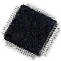
MC56F8257MLH Freescale Semiconductor, MC56F8257MLH Datasheet - Page 47

MC56F8257MLH
Manufacturer Part Number
MC56F8257MLH
Description
DSC 64K FLASH 60MHZ 64-LQFP
Manufacturer
Freescale Semiconductor
Series
56F8xxxr
Datasheets
1.TWR-56F8257.pdf
(88 pages)
2.MC56F8245VLD.pdf
(14 pages)
3.MC56F8245VLD.pdf
(2 pages)
4.MC56F8245VLD.pdf
(629 pages)
Specifications of MC56F8257MLH
Core Processor
56800E
Core Size
16-Bit
Speed
60MHz
Connectivity
CAN, I²C, LIN, SCI, SPI
Peripherals
LVD, POR, PWM, WDT
Number Of I /o
54
Program Memory Size
64KB (32K x 16)
Program Memory Type
FLASH
Ram Size
4K x 16
Voltage - Supply (vcc/vdd)
3 V ~ 3.6 V
Data Converters
A/D 16x12b, D/A 1x12b
Oscillator Type
Internal
Operating Temperature
-40°C ~ 105°C
Package / Case
64-LQFP
Product
DSCs
Processor Series
56800E
Core
56800E
Device Million Instructions Per Second
60 MIPs
Maximum Clock Frequency
60 MHz
Number Of Programmable I/os
54
Data Ram Size
8 KB
Operating Supply Voltage
3.3 V
Maximum Operating Temperature
+ 105 C
Mounting Style
SMD/SMT
Minimum Operating Temperature
- 40 C
On-chip Adc
12 bit, 8 Channel
Lead Free Status / RoHS Status
Lead free / RoHS Compliant
Eeprom Size
-
Lead Free Status / Rohs Status
Details
Available stocks
Company
Part Number
Manufacturer
Quantity
Price
Company:
Part Number:
MC56F8257MLH
Manufacturer:
MOTOLOLA
Quantity:
560
Company:
Part Number:
MC56F8257MLH
Manufacturer:
Freescale Semiconductor
Quantity:
10 000
- TWR-56F8257 PDF datasheet
- MC56F8245VLD PDF datasheet #2
- MC56F8245VLD PDF datasheet #3
- MC56F8245VLD PDF datasheet #4
- Current page: 47 of 629
- Download datasheet (4Mb)
2.3.1 ADC Control Register 1 (ADC_CTRL1)
Bits 14, 13, 12, and 11 in CTRL1 control all types of scans except parallel scans in the B
converter when CTRL2[SIMULT]=0. Non-simultaneous parallel scan modes allow
independent parallel scanning in the A and B converter. Bits 14, 13, 12, and 11 in CTRL2
are used to control B converter scans in non-simultaneous parallel scan modes.
Address: ADC_CTRL1 – F080h base + 0h offset = F080h
Freescale Semiconductor
Reset
Read
Write
Bit
Reserved
START0
STOP0
SYNC0
Field
15
14
13
12
15
0
0
14
1
This read-only bit is reserved and always has the value zero.
Stop
When this bit is asserted, the current scan is stopped and no further scans can start. Any further SYNC0
input pulses (see CTRL1[SYNC0] bit) or writes to the CTRL1[START0] bit are ignored until this bit has
been cleared. After the ADC is in stop mode, the results registers can be modified by the processor. Any
changes to the result registers in stop mode are treated as if the analog core supplied the data. Therefore,
limit checking, zero crossing, and associated interrupts can occur when authorized. This is not the same
as DSP STOP mode.
0
1
START0 Conversion
A scan is started by writing 1 to this bit. This is a write only bit. Writing 1 to it again while the scan remains
in process, is ignored.
The ADC must be in a stable power configuration prior to writing the start bit. Refer to the functional
description of power modes for further details.
0
1
SYNC0 Enable
A conversion may be initiated by asserting a positive edge on the SYNC0 input. Any subsequent SYNC0
input pulses while the scan remains in process are ignored unless the scan is awaiting furhter SYNC
inputs due to the SCTRL[SCn] bits. CTRL1[SYNC0] is cleared in ONCE mode, CTRL1[SMODE=000 or
001], when the first SYNC input is detected. This prevents unintentionally starting a new scan after the
first scan has completed.
START
Normal operation
Stop mode
No action
Start command is issued
13
0
0
12
1
MC56F825x/4x Reference Manual, Rev. 2, 10/2010
11
0
ADC_CTRL1 field descriptions
Table continues on the next page...
ZCIE
10
0
0
9
Preliminary
0
8
Description
0
7
CHNCFG_L
0
6
Chapter 2 Analog-to-Digital Converter (ADC)
0
5
0
4
0
0
3
1
2
SMODE
0
1
1
0
47
Related parts for MC56F8257MLH
Image
Part Number
Description
Manufacturer
Datasheet
Request
R
Part Number:
Description:
Manufacturer:
Freescale Semiconductor, Inc
Datasheet:
Part Number:
Description:
Manufacturer:
Freescale Semiconductor, Inc
Datasheet:
Part Number:
Description:
Manufacturer:
Freescale Semiconductor, Inc
Datasheet:
Part Number:
Description:
Manufacturer:
Freescale Semiconductor, Inc
Datasheet:
Part Number:
Description:
Manufacturer:
Freescale Semiconductor, Inc
Datasheet:
Part Number:
Description:
Manufacturer:
Freescale Semiconductor, Inc
Datasheet:
Part Number:
Description:
Manufacturer:
Freescale Semiconductor, Inc
Datasheet:
Part Number:
Description:
Manufacturer:
Freescale Semiconductor, Inc
Datasheet:
Part Number:
Description:
Manufacturer:
Freescale Semiconductor, Inc
Datasheet:
Part Number:
Description:
Manufacturer:
Freescale Semiconductor, Inc
Datasheet:
Part Number:
Description:
Manufacturer:
Freescale Semiconductor, Inc
Datasheet:
Part Number:
Description:
Manufacturer:
Freescale Semiconductor, Inc
Datasheet:
Part Number:
Description:
Manufacturer:
Freescale Semiconductor, Inc
Datasheet:
Part Number:
Description:
Manufacturer:
Freescale Semiconductor, Inc
Datasheet:
Part Number:
Description:
Manufacturer:
Freescale Semiconductor, Inc
Datasheet:


