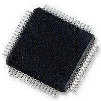
MC56F8257MLH Freescale Semiconductor, MC56F8257MLH Datasheet - Page 622

MC56F8257MLH
Manufacturer Part Number
MC56F8257MLH
Description
DSC 64K FLASH 60MHZ 64-LQFP
Manufacturer
Freescale Semiconductor
Series
56F8xxxr
Datasheets
1.TWR-56F8257.pdf
(88 pages)
2.MC56F8245VLD.pdf
(14 pages)
3.MC56F8245VLD.pdf
(2 pages)
4.MC56F8245VLD.pdf
(629 pages)
Specifications of MC56F8257MLH
Core Processor
56800E
Core Size
16-Bit
Speed
60MHz
Connectivity
CAN, I²C, LIN, SCI, SPI
Peripherals
LVD, POR, PWM, WDT
Number Of I /o
54
Program Memory Size
64KB (32K x 16)
Program Memory Type
FLASH
Ram Size
4K x 16
Voltage - Supply (vcc/vdd)
3 V ~ 3.6 V
Data Converters
A/D 16x12b, D/A 1x12b
Oscillator Type
Internal
Operating Temperature
-40°C ~ 105°C
Package / Case
64-LQFP
Product
DSCs
Processor Series
56800E
Core
56800E
Device Million Instructions Per Second
60 MIPs
Maximum Clock Frequency
60 MHz
Number Of Programmable I/os
54
Data Ram Size
8 KB
Operating Supply Voltage
3.3 V
Maximum Operating Temperature
+ 105 C
Mounting Style
SMD/SMT
Minimum Operating Temperature
- 40 C
On-chip Adc
12 bit, 8 Channel
Lead Free Status / RoHS Status
Lead free / RoHS Compliant
Eeprom Size
-
Lead Free Status / Rohs Status
Details
Available stocks
Company
Part Number
Manufacturer
Quantity
Price
Company:
Part Number:
MC56F8257MLH
Manufacturer:
MOTOLOLA
Quantity:
560
Company:
Part Number:
MC56F8257MLH
Manufacturer:
Freescale Semiconductor
Quantity:
10 000
- TWR-56F8257 PDF datasheet
- MC56F8245VLD PDF datasheet #2
- MC56F8245VLD PDF datasheet #3
- MC56F8245VLD PDF datasheet #4
- Current page: 622 of 629
- Download datasheet (4Mb)
External Signal Description
21.1.2 Block Diagram
21.2 External Signal Description
The following table summarizes the JTAG signals.
622
TCK
TDI
TMS
TDO
Pin
Test Clock Input — This input pin provides the clock to synchronize the test logic and shift serial data to
and from all TAP controllers and the TLM. If the EOnCE module is not being accessed using the master or
56800E core TAP controllers, the maximum TCK frequency is 1/4 the maximum frequency for the 56800E
core. When accessing the EOnCE module through the 56800E core TAP controller, the maximum frequen‐
cy for TCK is 1/8 the maximum frequency for the 56800E core. The TCK pin has a pulldown non-disabled
resistor.
Test Data Input — This input pin provides a serial input data stream to the TAP and the TLM. It is sampled
on the rising edge of TCK. TDI has an on-chip pullup resistor that can be disabled through PUPEN register
in the GPIO module.
Test Mode Select Input — This input pin is used to sequence the TAP controller’s TLM state machine. It is
sampled on the rising edge of TCK. TMS has an on-chip pullup resistor that can be disabled through PUP‐
EN register in the GPIO module. Note: Always tie the TMS pin to VDD through a 2.2K resistor.
Test Data Output — This three-state output pin provides a serial output data stream from the master TAP,
or 56800E core TAP controller. It is driven in the shift-IR and shift-DR controller states of the TAP control‐
ler state machines. Output data changes on the falling edge of TCK.
TMS
TCK
TDI
MC56F825x/4x Reference Manual, Rev. 2, 10/2010
Table 21-1. JTAG Pin Descriptions
Figure 21-1. JTAG Block Diagram
Boundary Scan Register
Instruction Decode
Instruction Register
FM Erase Register
IDCODE Register
Bypass Register
TLM TAP Select
Controller
TAP
Preliminary
Description
Freescale Semiconductor
TDO
Related parts for MC56F8257MLH
Image
Part Number
Description
Manufacturer
Datasheet
Request
R
Part Number:
Description:
Manufacturer:
Freescale Semiconductor, Inc
Datasheet:
Part Number:
Description:
Manufacturer:
Freescale Semiconductor, Inc
Datasheet:
Part Number:
Description:
Manufacturer:
Freescale Semiconductor, Inc
Datasheet:
Part Number:
Description:
Manufacturer:
Freescale Semiconductor, Inc
Datasheet:
Part Number:
Description:
Manufacturer:
Freescale Semiconductor, Inc
Datasheet:
Part Number:
Description:
Manufacturer:
Freescale Semiconductor, Inc
Datasheet:
Part Number:
Description:
Manufacturer:
Freescale Semiconductor, Inc
Datasheet:
Part Number:
Description:
Manufacturer:
Freescale Semiconductor, Inc
Datasheet:
Part Number:
Description:
Manufacturer:
Freescale Semiconductor, Inc
Datasheet:
Part Number:
Description:
Manufacturer:
Freescale Semiconductor, Inc
Datasheet:
Part Number:
Description:
Manufacturer:
Freescale Semiconductor, Inc
Datasheet:
Part Number:
Description:
Manufacturer:
Freescale Semiconductor, Inc
Datasheet:
Part Number:
Description:
Manufacturer:
Freescale Semiconductor, Inc
Datasheet:
Part Number:
Description:
Manufacturer:
Freescale Semiconductor, Inc
Datasheet:
Part Number:
Description:
Manufacturer:
Freescale Semiconductor, Inc
Datasheet:


