MC56F8257MLH Freescale Semiconductor, MC56F8257MLH Datasheet - Page 3
MC56F8257MLH
Manufacturer Part Number
MC56F8257MLH
Description
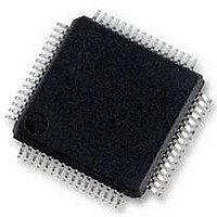
DSC 64K FLASH 60MHZ 64-LQFP
Manufacturer
Freescale Semiconductor
Series
56F8xxxr
Datasheets
1.TWR-56F8257.pdf
(88 pages)
2.MC56F8245VLD.pdf
(14 pages)
3.MC56F8245VLD.pdf
(2 pages)
4.MC56F8245VLD.pdf
(629 pages)
Specifications of MC56F8257MLH
Core Processor
56800E
Core Size
16-Bit
Speed
60MHz
Connectivity
CAN, I²C, LIN, SCI, SPI
Peripherals
LVD, POR, PWM, WDT
Number Of I /o
54
Program Memory Size
64KB (32K x 16)
Program Memory Type
FLASH
Ram Size
4K x 16
Voltage - Supply (vcc/vdd)
3 V ~ 3.6 V
Data Converters
A/D 16x12b, D/A 1x12b
Oscillator Type
Internal
Operating Temperature
-40°C ~ 105°C
Package / Case
64-LQFP
Product
DSCs
Processor Series
56800E
Core
56800E
Device Million Instructions Per Second
60 MIPs
Maximum Clock Frequency
60 MHz
Number Of Programmable I/os
54
Data Ram Size
8 KB
Operating Supply Voltage
3.3 V
Maximum Operating Temperature
+ 105 C
Mounting Style
SMD/SMT
Minimum Operating Temperature
- 40 C
On-chip Adc
12 bit, 8 Channel
Lead Free Status / RoHS Status
Lead free / RoHS Compliant
Eeprom Size
-
Lead Free Status / Rohs Status
Details
Available stocks
Company
Part Number
Manufacturer
Quantity
Price
Company:

Part Number:
MC56F8257MLH
Manufacturer:
MOTOLOLA
Quantity:
560
Company:
Part Number:
MC56F8257MLH
Manufacturer:
Freescale Semiconductor
Quantity:
10 000


Section Number
1.1
1.2
1.3
1.4
1.5
2.1
2.2
2.3
Freescale Semiconductor
Introduction.....................................................................................................................................................................31
Features...........................................................................................................................................................................31
Core Block Diagram.......................................................................................................................................................34
Peripheral Subsystem......................................................................................................................................................35
Clock Generation and Distribution.................................................................................................................................37
Introduction.....................................................................................................................................................................39
2.1.1
2.1.2
2.1.3
Signal Descriptions.........................................................................................................................................................41
2.2.1
2.2.2
Memory Map and Registers............................................................................................................................................43
2.3.1
2.3.2
2.3.3
2.3.4
2.3.5
2.3.6
2.3.7
2.3.8
2.3.9
Overview..........................................................................................................................................................39
Features............................................................................................................................................................39
Block Diagram.................................................................................................................................................40
Overview..........................................................................................................................................................41
External Signal Descriptions............................................................................................................................41
2.2.2.1
2.2.2.2
ADC Control Register 1 (ADCCTRL1)..........................................................................................................47
ADC Control Register 2 (ADCCTRL2)..........................................................................................................50
ADC Zero Crossing Control Register (ADCZXCTRL)..................................................................................53
ADC Channel List Register 1 (ADCCLIST1).................................................................................................54
ADC Channel List Register 2 (ADCCLIST2).................................................................................................56
ADC Channel List Register 3 (ADCCLIST3).................................................................................................58
ADC Channel List Register 4 (ADCCLIST4).................................................................................................60
ADC Sample Disable Register (ADCSDIS)....................................................................................................62
ADC Status Register (ADCSTAT)..................................................................................................................62
Analog Input Pins (ANA[0:7] and ANB[0:7])..............................................................................41
Voltage Reference Pins (VREFH and VREFLO)..........................................................................42
MC56F825x/4x Reference Manual, Rev. 2, 10/2010
Analog-to-Digital Converter (ADC)
Device Overview
Contents
Chapter 1
Chapter 2
Preliminary
Title
Page
3
Related parts for MC56F8257MLH
Image
Part Number
Description
Manufacturer
Datasheet
Request
R

Part Number:
Description:
Manufacturer:
Freescale Semiconductor, Inc
Datasheet:
Part Number:
Description:
Manufacturer:
Freescale Semiconductor, Inc
Datasheet:
Part Number:
Description:
Manufacturer:
Freescale Semiconductor, Inc
Datasheet:
Part Number:
Description:
Manufacturer:
Freescale Semiconductor, Inc
Datasheet:
Part Number:
Description:
Manufacturer:
Freescale Semiconductor, Inc
Datasheet:
Part Number:
Description:
Manufacturer:
Freescale Semiconductor, Inc
Datasheet:
Part Number:
Description:
Manufacturer:
Freescale Semiconductor, Inc
Datasheet:
Part Number:
Description:
Manufacturer:
Freescale Semiconductor, Inc
Datasheet:
Part Number:
Description:
Manufacturer:
Freescale Semiconductor, Inc
Datasheet:
Part Number:
Description:
Manufacturer:
Freescale Semiconductor, Inc
Datasheet:
Part Number:
Description:
Manufacturer:
Freescale Semiconductor, Inc
Datasheet:
Part Number:
Description:
Manufacturer:
Freescale Semiconductor, Inc
Datasheet:
Part Number:
Description:
Manufacturer:
Freescale Semiconductor, Inc
Datasheet:
Part Number:
Description:
Manufacturer:
Freescale Semiconductor, Inc
Datasheet:
Part Number:
Description:
Manufacturer:
Freescale Semiconductor, Inc
Datasheet: