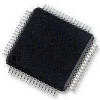
MC56F8257MLH Freescale Semiconductor, MC56F8257MLH Datasheet - Page 404

MC56F8257MLH
Manufacturer Part Number
MC56F8257MLH
Description
DSC 64K FLASH 60MHZ 64-LQFP
Manufacturer
Freescale Semiconductor
Series
56F8xxxr
Datasheets
1.TWR-56F8257.pdf
(88 pages)
2.MC56F8245VLD.pdf
(14 pages)
3.MC56F8245VLD.pdf
(2 pages)
4.MC56F8245VLD.pdf
(629 pages)
Specifications of MC56F8257MLH
Core Processor
56800E
Core Size
16-Bit
Speed
60MHz
Connectivity
CAN, I²C, LIN, SCI, SPI
Peripherals
LVD, POR, PWM, WDT
Number Of I /o
54
Program Memory Size
64KB (32K x 16)
Program Memory Type
FLASH
Ram Size
4K x 16
Voltage - Supply (vcc/vdd)
3 V ~ 3.6 V
Data Converters
A/D 16x12b, D/A 1x12b
Oscillator Type
Internal
Operating Temperature
-40°C ~ 105°C
Package / Case
64-LQFP
Product
DSCs
Processor Series
56800E
Core
56800E
Device Million Instructions Per Second
60 MIPs
Maximum Clock Frequency
60 MHz
Number Of Programmable I/os
54
Data Ram Size
8 KB
Operating Supply Voltage
3.3 V
Maximum Operating Temperature
+ 105 C
Mounting Style
SMD/SMT
Minimum Operating Temperature
- 40 C
On-chip Adc
12 bit, 8 Channel
Lead Free Status / RoHS Status
Lead free / RoHS Compliant
Eeprom Size
-
Lead Free Status / Rohs Status
Details
Available stocks
Company
Part Number
Manufacturer
Quantity
Price
Company:
Part Number:
MC56F8257MLH
Manufacturer:
MOTOLOLA
Quantity:
560
Company:
Part Number:
MC56F8257MLH
Manufacturer:
Freescale Semiconductor
Quantity:
10 000
- TWR-56F8257 PDF datasheet
- MC56F8245VLD PDF datasheet #2
- MC56F8245VLD PDF datasheet #3
- MC56F8245VLD PDF datasheet #4
- Current page: 404 of 629
- Download datasheet (4Mb)
Operating Modes
>
12.4.2.4 Transaction Format When CPHA = 0
The following figure shows an SPI transaction in which CPHA is logic zero. The figure
should not be used as a replacement for data sheet parametric information. It assumes 16
bit data lengths and the MSB shifted out first.
Two waveforms are shown for SCLK: one for CPOL = 0 and another for CPOL = 1. The
diagram may be interpreted as a master or slave timing diagram since the serial clock
(SCLK), master in/slave out (MISO), and master out/slave in (MOSI) pins are directly
connected between the master and the slave. The MISO signal is the output from the
slave, and the MOSI signal is the output from the master. When CPHA = 0, the first
SCLK edge is the MSB capture strobe. Therefore, the slave must begin driving its data
before the first SCLK edge, and a falling edge on the SS pin is used to start the slave data
transaction. The slave SS pin must be toggled back to high and then low again between
each data word transmitted, as shown in the following figure.
404
Before writing to the CPOL bit or the CPHA bit, disable the
SPI by clearing the SPI enable bit (SPE).
Figure 12-10. Transaction Format (CPHA = 0)
MC56F825x/4x Reference Manual, Rev. 2, 10/2010
Preliminary
Note
Freescale Semiconductor
Related parts for MC56F8257MLH
Image
Part Number
Description
Manufacturer
Datasheet
Request
R
Part Number:
Description:
Manufacturer:
Freescale Semiconductor, Inc
Datasheet:
Part Number:
Description:
Manufacturer:
Freescale Semiconductor, Inc
Datasheet:
Part Number:
Description:
Manufacturer:
Freescale Semiconductor, Inc
Datasheet:
Part Number:
Description:
Manufacturer:
Freescale Semiconductor, Inc
Datasheet:
Part Number:
Description:
Manufacturer:
Freescale Semiconductor, Inc
Datasheet:
Part Number:
Description:
Manufacturer:
Freescale Semiconductor, Inc
Datasheet:
Part Number:
Description:
Manufacturer:
Freescale Semiconductor, Inc
Datasheet:
Part Number:
Description:
Manufacturer:
Freescale Semiconductor, Inc
Datasheet:
Part Number:
Description:
Manufacturer:
Freescale Semiconductor, Inc
Datasheet:
Part Number:
Description:
Manufacturer:
Freescale Semiconductor, Inc
Datasheet:
Part Number:
Description:
Manufacturer:
Freescale Semiconductor, Inc
Datasheet:
Part Number:
Description:
Manufacturer:
Freescale Semiconductor, Inc
Datasheet:
Part Number:
Description:
Manufacturer:
Freescale Semiconductor, Inc
Datasheet:
Part Number:
Description:
Manufacturer:
Freescale Semiconductor, Inc
Datasheet:
Part Number:
Description:
Manufacturer:
Freescale Semiconductor, Inc
Datasheet:


