MC56F8257MLH Freescale Semiconductor, MC56F8257MLH Datasheet - Page 209
MC56F8257MLH
Manufacturer Part Number
MC56F8257MLH
Description
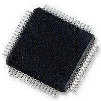
DSC 64K FLASH 60MHZ 64-LQFP
Manufacturer
Freescale Semiconductor
Series
56F8xxxr
Datasheets
1.TWR-56F8257.pdf
(88 pages)
2.MC56F8245VLD.pdf
(14 pages)
3.MC56F8245VLD.pdf
(2 pages)
4.MC56F8245VLD.pdf
(629 pages)
Specifications of MC56F8257MLH
Core Processor
56800E
Core Size
16-Bit
Speed
60MHz
Connectivity
CAN, I²C, LIN, SCI, SPI
Peripherals
LVD, POR, PWM, WDT
Number Of I /o
54
Program Memory Size
64KB (32K x 16)
Program Memory Type
FLASH
Ram Size
4K x 16
Voltage - Supply (vcc/vdd)
3 V ~ 3.6 V
Data Converters
A/D 16x12b, D/A 1x12b
Oscillator Type
Internal
Operating Temperature
-40°C ~ 105°C
Package / Case
64-LQFP
Product
DSCs
Processor Series
56800E
Core
56800E
Device Million Instructions Per Second
60 MIPs
Maximum Clock Frequency
60 MHz
Number Of Programmable I/os
54
Data Ram Size
8 KB
Operating Supply Voltage
3.3 V
Maximum Operating Temperature
+ 105 C
Mounting Style
SMD/SMT
Minimum Operating Temperature
- 40 C
On-chip Adc
12 bit, 8 Channel
Lead Free Status / RoHS Status
Lead free / RoHS Compliant
Eeprom Size
-
Lead Free Status / Rohs Status
Details
Available stocks
Company
Part Number
Manufacturer
Quantity
Price
Company:

Part Number:
MC56F8257MLH
Manufacturer:
MOTOLOLA
Quantity:
560
Company:
Part Number:
MC56F8257MLH
Manufacturer:
Freescale Semiconductor
Quantity:
10 000


7.3.5 PWM SMx Value Register 0 (PWM_SMnVAL0)
Addresses: PWM_SM0VAL0 – F300h base + 5h offset = F305h
7.3.6 PWM SMx Fractional Value Register 1 (PWM_SMnFRACVAL1)
Addresses: PWM_SM0FRACVAL1 – F300h base + 6h offset = F306h
Freescale Semiconductor
Reset
Reset
Read
Read
Write
Write
Bit
Bit
DBLEN
VAL0
15–0
Field
Field
0
15
15
0
0
PWM_SM1VAL0 – F300h base + 35h offset = F335h
PWM_SM2VAL0 – F300h base + 65h offset = F365h
PWM_SM1FRACVAL1 – F300h base + 36h offset = F336h
PWM_SM2FRACVAL1 – F300h base + 66h offset = F366h
14
14
0
0
Double Switching Enable
This read/write bit enables the double switching PWM behavior.
0
1
Value Register 0
The 16-bit signed value in this buffered, read/write register defines the mid-cycle reload point for the PWM
in PWM clock periods. This value also defines when the PWMX signal is set and the local sync signal is
reset. This register is not byte accessible.
NOTE: The VAL0 register is buffered. The value written does not take effect until MCTRL[LDOK] is set
FRACVAL1
Double switching disabled.
Double switching enabled.
13
13
0
0
and the next PWM load cycle begins or CTRL[LDMOD] is set. VAL0 cannot be written when
MCTRL[LDOK] is set. Reading VAL0 reads the value in a buffer. It is not necessarily the value
the PWM generator is currently using.
PWM_SMnCTRL field descriptions (continued)
12
12
0
0
MC56F825x/4x Reference Manual, Rev. 2, 10/2010
PWM_SMnVAL0 field descriptions
11
11
0
0
10
10
0
0
0
0
9
9
Preliminary
Chapter 7 Enhanced Flex Pulse Width Modulator (eFlexPWM)
0
0
8
8
VAL0
Description
Description
0
0
7
7
0
0
6
6
0
0
0
5
5
0
0
4
4
0
0
3
3
0
0
2
2
0
0
1
1
0
0
0
0
209
Related parts for MC56F8257MLH
Image
Part Number
Description
Manufacturer
Datasheet
Request
R

Part Number:
Description:
Manufacturer:
Freescale Semiconductor, Inc
Datasheet:
Part Number:
Description:
Manufacturer:
Freescale Semiconductor, Inc
Datasheet:
Part Number:
Description:
Manufacturer:
Freescale Semiconductor, Inc
Datasheet:
Part Number:
Description:
Manufacturer:
Freescale Semiconductor, Inc
Datasheet:
Part Number:
Description:
Manufacturer:
Freescale Semiconductor, Inc
Datasheet:
Part Number:
Description:
Manufacturer:
Freescale Semiconductor, Inc
Datasheet:
Part Number:
Description:
Manufacturer:
Freescale Semiconductor, Inc
Datasheet:
Part Number:
Description:
Manufacturer:
Freescale Semiconductor, Inc
Datasheet:
Part Number:
Description:
Manufacturer:
Freescale Semiconductor, Inc
Datasheet:
Part Number:
Description:
Manufacturer:
Freescale Semiconductor, Inc
Datasheet:
Part Number:
Description:
Manufacturer:
Freescale Semiconductor, Inc
Datasheet:
Part Number:
Description:
Manufacturer:
Freescale Semiconductor, Inc
Datasheet:
Part Number:
Description:
Manufacturer:
Freescale Semiconductor, Inc
Datasheet:
Part Number:
Description:
Manufacturer:
Freescale Semiconductor, Inc
Datasheet:
Part Number:
Description:
Manufacturer:
Freescale Semiconductor, Inc
Datasheet: