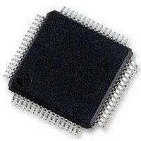
MC56F8257MLH Freescale Semiconductor, MC56F8257MLH Datasheet - Page 610

MC56F8257MLH
Manufacturer Part Number
MC56F8257MLH
Description
DSC 64K FLASH 60MHZ 64-LQFP
Manufacturer
Freescale Semiconductor
Series
56F8xxxr
Datasheets
1.TWR-56F8257.pdf
(88 pages)
2.MC56F8245VLD.pdf
(14 pages)
3.MC56F8245VLD.pdf
(2 pages)
4.MC56F8245VLD.pdf
(629 pages)
Specifications of MC56F8257MLH
Core Processor
56800E
Core Size
16-Bit
Speed
60MHz
Connectivity
CAN, I²C, LIN, SCI, SPI
Peripherals
LVD, POR, PWM, WDT
Number Of I /o
54
Program Memory Size
64KB (32K x 16)
Program Memory Type
FLASH
Ram Size
4K x 16
Voltage - Supply (vcc/vdd)
3 V ~ 3.6 V
Data Converters
A/D 16x12b, D/A 1x12b
Oscillator Type
Internal
Operating Temperature
-40°C ~ 105°C
Package / Case
64-LQFP
Product
DSCs
Processor Series
56800E
Core
56800E
Device Million Instructions Per Second
60 MIPs
Maximum Clock Frequency
60 MHz
Number Of Programmable I/os
54
Data Ram Size
8 KB
Operating Supply Voltage
3.3 V
Maximum Operating Temperature
+ 105 C
Mounting Style
SMD/SMT
Minimum Operating Temperature
- 40 C
On-chip Adc
12 bit, 8 Channel
Lead Free Status / RoHS Status
Lead free / RoHS Compliant
Eeprom Size
-
Lead Free Status / Rohs Status
Details
Available stocks
Company
Part Number
Manufacturer
Quantity
Price
Company:
Part Number:
MC56F8257MLH
Manufacturer:
MOTOLOLA
Quantity:
560
Company:
Part Number:
MC56F8257MLH
Manufacturer:
Freescale Semiconductor
Quantity:
10 000
- TWR-56F8257 PDF datasheet
- MC56F8245VLD PDF datasheet #2
- MC56F8245VLD PDF datasheet #3
- MC56F8245VLD PDF datasheet #4
- Current page: 610 of 629
- Download datasheet (4Mb)
Functional Description
20.3.1 Read Operation
The embedded flash memory module provides transparent read access to all memory
locations in its flash data array. Each read is achieved without wait states, providing
memory access without delays. Read operations execute through either instruction
fetches or 56800E program memory read instructions.
20.3.2 Write Operation
Normal write access, where a value is written to a memory location within the program
flash memory array, is part of a programming attempt. Writing the data must be followed
by writing a program command to the HFM module’s command register. Address and
data in a 56800E program memory write instruction specifies the desired location and
data to be programmed. To launch the module's state machine to process and effect the
write:
The flash command register and address and data buffer operate as a two-stage FIFO.
Consequently, a new command, along with the necessary data and address, can be stored
in the buffer while the previous command is still in progress. This technique can be
applied to all commands except RDARYM and RDARYMI. A new command can be
buffered only if the buffer is empty, which is indicated when the CBEIF flag in the user
status register reads 0; otherwise the attempt to launch the new command will be flagged
as an error. This feature increases the rate at which the HFM state machine receives
commands, reducing command processing time, and expedites program/erase cycles.
Another flag in the flash user status register signals command completion. Interrupts are
generated when they are enabled.
Erased flash consists of all ones, so any programming attempt writes only the required
zeros to create the desired bit pattern. The user must verify the erased state of the
destination in flash before programming it.
20.3.3 Erase Operation
To perform an erase operation:
610
1. Execute a program memory write instruction.
2. Write the program command code (0020h) to the command register.
3. Write 1 to the CBEIF bit.
MC56F825x/4x Reference Manual, Rev. 2, 10/2010
Preliminary
Freescale Semiconductor
Related parts for MC56F8257MLH
Image
Part Number
Description
Manufacturer
Datasheet
Request
R
Part Number:
Description:
Manufacturer:
Freescale Semiconductor, Inc
Datasheet:
Part Number:
Description:
Manufacturer:
Freescale Semiconductor, Inc
Datasheet:
Part Number:
Description:
Manufacturer:
Freescale Semiconductor, Inc
Datasheet:
Part Number:
Description:
Manufacturer:
Freescale Semiconductor, Inc
Datasheet:
Part Number:
Description:
Manufacturer:
Freescale Semiconductor, Inc
Datasheet:
Part Number:
Description:
Manufacturer:
Freescale Semiconductor, Inc
Datasheet:
Part Number:
Description:
Manufacturer:
Freescale Semiconductor, Inc
Datasheet:
Part Number:
Description:
Manufacturer:
Freescale Semiconductor, Inc
Datasheet:
Part Number:
Description:
Manufacturer:
Freescale Semiconductor, Inc
Datasheet:
Part Number:
Description:
Manufacturer:
Freescale Semiconductor, Inc
Datasheet:
Part Number:
Description:
Manufacturer:
Freescale Semiconductor, Inc
Datasheet:
Part Number:
Description:
Manufacturer:
Freescale Semiconductor, Inc
Datasheet:
Part Number:
Description:
Manufacturer:
Freescale Semiconductor, Inc
Datasheet:
Part Number:
Description:
Manufacturer:
Freescale Semiconductor, Inc
Datasheet:
Part Number:
Description:
Manufacturer:
Freescale Semiconductor, Inc
Datasheet:


