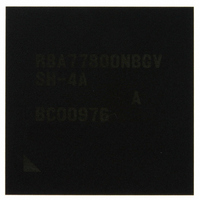
R8A77800ANBGAV Renesas Electronics America, R8A77800ANBGAV Datasheet - Page 671

R8A77800ANBGAV
Manufacturer Part Number
R8A77800ANBGAV
Description
IC SUPERH MPU ROMLESS 449-BGA
Manufacturer
Renesas Electronics America
Series
SuperH® SH7780r
Datasheet
1.R8A77800ANBGV.pdf
(1342 pages)
Specifications of R8A77800ANBGAV
Core Processor
SH-4A
Core Size
32-Bit
Speed
400MHz
Connectivity
Audio Codec, MMC, Serial Sound, SCI, SIO, SPI, SSI
Peripherals
DMA, POR, WDT
Number Of I /o
75
Program Memory Type
ROMless
Ram Size
16K x 8
Voltage - Supply (vcc/vdd)
1.15 V ~ 1.35 V
Oscillator Type
External
Operating Temperature
-20°C ~ 75°C
Package / Case
449-BGA
Lead Free Status / RoHS Status
Lead free / RoHS Compliant
Eeprom Size
-
Program Memory Size
-
Data Converters
-
Available stocks
Company
Part Number
Manufacturer
Quantity
Price
Company:
Part Number:
R8A77800ANBGAV
Manufacturer:
Renesas Electronics America
Quantity:
10 000
- Current page: 671 of 1342
- Download datasheet (7Mb)
15.4.1
FRQCR is a 32-bit readable/writable register that selects the frequency division ratio of the
SuperHyway clock (SHck), the peripheral clock (Pck), the DDR clock (DDRck) and the bus clock
(Bck). Refer to the clock operating mode table about the frequency multiplication ratio. FRQCR
can only be accessed in longwords. FRQCR is initialized by a power-on reset via the PRESET pin
and WDT over-flow.
Initial value:
Initial value:
Bit
31 to 28
27 to 25
24
23
22
21
20
Note: The initial values of these fields after power-on reset depend on the mode pins setting (see table 15.2).
R/W:
R/W:
BIt:
BIt:
Frequency Control Register (FRQCR)
Bit Name
IFC0*
CFC3*
CFC2*
CFC1*
CFC0*
31
15
R
R
0
0
30
14
R
R
0
29
13
R
R
0
Initial
Value
0001
000
Undefined R/W
0
Undefined
Undefined
0
28
12
R
R
1
27
11
R
R
0
0
R/W
R
R
R/W
26
10
R
R
0
0
Description
Reserved
These bits are always read as 0001. The write value
should always be 0001.
Reserved
These bits are always read as 0. The write value
should always be 0.
Writing to other than 000, the operation of this LSI is
not guaranteed.
CPU Clock (Ick) and SuperHyway Clock (SHck)
Frequency Division Ratio Setting
00010: ×12 (Ick), ×6 (SHck) Clock operating mode 0, 1,
00100: ×12 (Ick), ×4 (SHck) Clock operating mode 12
10000: ×6 (Ick), ×6 (SHck) Register setting
Other than above: Setting prohibited
The initial value of this field after power-on reset
depends on the mode pins setting (see table 15.2).
25
R
R
0
9
1
IFC0*
R/W
(register setting after initialized)
(after power-on reset)
2 or 3 (after power-on reset)
24
R
8
1
R/W
23
R
0
7
0
Rev.1.00 Dec. 13, 2005 Page 619 of 1286
R/W
Section 15 Clock Pulse Generator (CPG)
22
CFC[3:0]*
R
6
R/W
21
R
5
R/W
20
R
0
4
19
R
R
0
3
0
REJ09B0158-0100
P1FC[3:0]*
18
BFC[3:0]*
R
R
2
1
17
R
R
1
16
R
R
0
Related parts for R8A77800ANBGAV
Image
Part Number
Description
Manufacturer
Datasheet
Request
R

Part Number:
Description:
KIT STARTER FOR M16C/29
Manufacturer:
Renesas Electronics America
Datasheet:

Part Number:
Description:
KIT STARTER FOR R8C/2D
Manufacturer:
Renesas Electronics America
Datasheet:

Part Number:
Description:
R0K33062P STARTER KIT
Manufacturer:
Renesas Electronics America
Datasheet:

Part Number:
Description:
KIT STARTER FOR R8C/23 E8A
Manufacturer:
Renesas Electronics America
Datasheet:

Part Number:
Description:
KIT STARTER FOR R8C/25
Manufacturer:
Renesas Electronics America
Datasheet:

Part Number:
Description:
KIT STARTER H8S2456 SHARPE DSPLY
Manufacturer:
Renesas Electronics America
Datasheet:

Part Number:
Description:
KIT STARTER FOR R8C38C
Manufacturer:
Renesas Electronics America
Datasheet:

Part Number:
Description:
KIT STARTER FOR R8C35C
Manufacturer:
Renesas Electronics America
Datasheet:

Part Number:
Description:
KIT STARTER FOR R8CL3AC+LCD APPS
Manufacturer:
Renesas Electronics America
Datasheet:

Part Number:
Description:
KIT STARTER FOR RX610
Manufacturer:
Renesas Electronics America
Datasheet:

Part Number:
Description:
KIT STARTER FOR R32C/118
Manufacturer:
Renesas Electronics America
Datasheet:

Part Number:
Description:
KIT DEV RSK-R8C/26-29
Manufacturer:
Renesas Electronics America
Datasheet:

Part Number:
Description:
KIT STARTER FOR SH7124
Manufacturer:
Renesas Electronics America
Datasheet:

Part Number:
Description:
KIT STARTER FOR H8SX/1622
Manufacturer:
Renesas Electronics America
Datasheet:

Part Number:
Description:
KIT DEV FOR SH7203
Manufacturer:
Renesas Electronics America
Datasheet:


