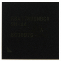
R8A77800ANBGAV Renesas Electronics America, R8A77800ANBGAV Datasheet - Page 392

R8A77800ANBGAV
Manufacturer Part Number
R8A77800ANBGAV
Description
IC SUPERH MPU ROMLESS 449-BGA
Manufacturer
Renesas Electronics America
Series
SuperH® SH7780r
Datasheet
1.R8A77800ANBGV.pdf
(1342 pages)
Specifications of R8A77800ANBGAV
Core Processor
SH-4A
Core Size
32-Bit
Speed
400MHz
Connectivity
Audio Codec, MMC, Serial Sound, SCI, SIO, SPI, SSI
Peripherals
DMA, POR, WDT
Number Of I /o
75
Program Memory Type
ROMless
Ram Size
16K x 8
Voltage - Supply (vcc/vdd)
1.15 V ~ 1.35 V
Oscillator Type
External
Operating Temperature
-20°C ~ 75°C
Package / Case
449-BGA
Lead Free Status / RoHS Status
Lead free / RoHS Compliant
Eeprom Size
-
Program Memory Size
-
Data Converters
-
Available stocks
Company
Part Number
Manufacturer
Quantity
Price
Company:
Part Number:
R8A77800ANBGAV
Manufacturer:
Renesas Electronics America
Quantity:
10 000
- Current page: 392 of 1342
- Download datasheet (7Mb)
Section 11 Local Bus State Controller (LBSC)
Rev.1.00 Dec. 13, 2005 Page 340 of 1286
REJ09B0158-0100
Bit
9, 8
7
6 to 4
Bit Name
SZ
RDSPL
BW
Initial
Value
11
0
111
R/W
R/W*
R/W
R/W
Description
Bus Width
Specify the bus width. Set to 11 for the MPX interface,
and set to 10 or 11 for the byte control SRAM interface.
In CS0BCR, the external pins (MODE3 and MODE4)
are sampled at a power-on reset.
00: Reserved
01: 8 bits
10: 16 bits
11: 32 bits
Note: * Bits SZ in CS0BCR are read-only. The SZ bits
RD Hold Cycle
Specifies the number of cycles to be inserted into the
RD assertion period to elongate the data hold time for
the read data sample timing. When setting this bit to 1,
specify the number of RD negation-CSn negation delay
cycles as 1 or more by setting the RDH bit in CSnWCR.
Also the RD negation-CSn negation delay cycle is
reduced by 1 cycle when this bit is set to 1 (Available
only when the SRAM interface or byte control SRAM
interface).
0: No hold cycle inserted
1: 1 hold cycle inserted
Burst Pitch
When the burst ROM interface is used, these bits
specify the number of wait cycles to be inserted after
the second data access in a burst transfer.
000: No idle cycle inserted, RDY signal disabled
001: 1 idle cycle inserted, RDY signal enabled
010: 2 idle cycles inserted, RDY signal enabled
011: 3 idle cycles inserted, RDY signal enabled
100: 4 idle cycles inserted, RDY signal enabled
101: 5 idle cycles inserted, RDY signal enabled
110: 6 idle cycles inserted, RDY signal enabled
111: 7 idle cycles inserted, RDY signal enabled
in CS0BCR are set to 11 when area 0 is set to
the MPX interface by the MODE3 and MODE4
pins.
Related parts for R8A77800ANBGAV
Image
Part Number
Description
Manufacturer
Datasheet
Request
R

Part Number:
Description:
KIT STARTER FOR M16C/29
Manufacturer:
Renesas Electronics America
Datasheet:

Part Number:
Description:
KIT STARTER FOR R8C/2D
Manufacturer:
Renesas Electronics America
Datasheet:

Part Number:
Description:
R0K33062P STARTER KIT
Manufacturer:
Renesas Electronics America
Datasheet:

Part Number:
Description:
KIT STARTER FOR R8C/23 E8A
Manufacturer:
Renesas Electronics America
Datasheet:

Part Number:
Description:
KIT STARTER FOR R8C/25
Manufacturer:
Renesas Electronics America
Datasheet:

Part Number:
Description:
KIT STARTER H8S2456 SHARPE DSPLY
Manufacturer:
Renesas Electronics America
Datasheet:

Part Number:
Description:
KIT STARTER FOR R8C38C
Manufacturer:
Renesas Electronics America
Datasheet:

Part Number:
Description:
KIT STARTER FOR R8C35C
Manufacturer:
Renesas Electronics America
Datasheet:

Part Number:
Description:
KIT STARTER FOR R8CL3AC+LCD APPS
Manufacturer:
Renesas Electronics America
Datasheet:

Part Number:
Description:
KIT STARTER FOR RX610
Manufacturer:
Renesas Electronics America
Datasheet:

Part Number:
Description:
KIT STARTER FOR R32C/118
Manufacturer:
Renesas Electronics America
Datasheet:

Part Number:
Description:
KIT DEV RSK-R8C/26-29
Manufacturer:
Renesas Electronics America
Datasheet:

Part Number:
Description:
KIT STARTER FOR SH7124
Manufacturer:
Renesas Electronics America
Datasheet:

Part Number:
Description:
KIT STARTER FOR H8SX/1622
Manufacturer:
Renesas Electronics America
Datasheet:

Part Number:
Description:
KIT DEV FOR SH7203
Manufacturer:
Renesas Electronics America
Datasheet:


