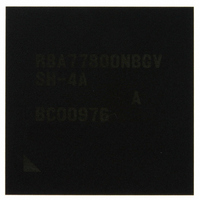
R8A77800ANBGAV Renesas Electronics America, R8A77800ANBGAV Datasheet - Page 41

R8A77800ANBGAV
Manufacturer Part Number
R8A77800ANBGAV
Description
IC SUPERH MPU ROMLESS 449-BGA
Manufacturer
Renesas Electronics America
Series
SuperH® SH7780r
Datasheet
1.R8A77800ANBGV.pdf
(1342 pages)
Specifications of R8A77800ANBGAV
Core Processor
SH-4A
Core Size
32-Bit
Speed
400MHz
Connectivity
Audio Codec, MMC, Serial Sound, SCI, SIO, SPI, SSI
Peripherals
DMA, POR, WDT
Number Of I /o
75
Program Memory Type
ROMless
Ram Size
16K x 8
Voltage - Supply (vcc/vdd)
1.15 V ~ 1.35 V
Oscillator Type
External
Operating Temperature
-20°C ~ 75°C
Package / Case
449-BGA
Lead Free Status / RoHS Status
Lead free / RoHS Compliant
Eeprom Size
-
Program Memory Size
-
Data Converters
-
Available stocks
Company
Part Number
Manufacturer
Quantity
Price
Company:
Part Number:
R8A77800ANBGAV
Manufacturer:
Renesas Electronics America
Quantity:
10 000
- Current page: 41 of 1342
- Download datasheet (7Mb)
Figure 25.5 Sample Flowchart for Off-Chip Codec Register Read (1) ...................................... 978
Figure 25.6 Sample Flowchart for Off-Chip Codec Register Read (2) ...................................... 979
Figure 25.7 Sample Flowchart for Off-Chip Codec Register Read (3) ...................................... 980
Section 26 Serial Sound Interface (SSI) Module
Figure 26.1 Block Diagram of SSI Module ................................................................................ 984
Figure 26.2 Philips Format (with no Padding).......................................................................... 1000
Figure 26.3 Philips Format (with Padding)............................................................................... 1000
Figure 26.4 Sony Format (with Serial Data First, Followed by Padding Bits) ......................... 1001
Figure 26.5 Matsushita Format (with Padding Bits First, Followed by Serial Data)................ 1001
Figure 26.6 Multi-channel Format (4 Channels, No Padding).................................................. 1003
Figure 26.7 Multi-channel Format (6 Channels with High Padding) ....................................... 1003
Figure 26.8 Multi-channel Format (8 Channels, with Padding Bits First,
Figure 26.9 Basic Sample Format
Figure 26.10 Inverted Clock ..................................................................................................... 1005
Figure 26.11 Inverted Word Select........................................................................................... 1006
Figure 26.12 Inverted Padding Polarity .................................................................................... 1006
Figure 26.13 Padding Bits First, Followed by Serial Data, with Delay.................................... 1006
Figure 26.14 Padding Bits First, Followed by Serial Data, without Delay............................... 1007
Figure 26.15 Serial Data First, Followed by Padding Bits, without Delay............................... 1007
Figure 26.16 Parallel Right Aligned with Delay....................................................................... 1007
Figure 26.17 Mute Enabled ...................................................................................................... 1008
Figure 26.18 Compressed Data Format, Slave Transmitter, Burst Mode Disabled .................. 1009
Figure 26.19 Compressed Data Format, Slave Transmitter, and Burst Mode Enabled ............ 1009
Figure 26.20 Transition Diagram between Operation Modes................................................... 1011
Figure 26.21 Transmission Using DMA Controller ................................................................. 1013
Figure 26.22 Transmission using Interrupt Data Flow Control ................................................ 1014
Figure 26.23 Reception using DMA Controller........................................................................ 1016
Figure 26.24 Reception using Interrupt Data Flow Control ..................................................... 1017
Section 27 NAND Flash Memory Controller (FLCTL)
Figure 27.1 FLCTL Block Diagram ......................................................................................... 1023
Figure 27.2 Read Operation Timing for NAND-Type Flash Memory (1)................................ 1044
Figure 27.3 Programming Operation Timing for NAND-Type Flash Memory (1) .................. 1045
Figure 27.4 Programming Operation Timing for NAND-Type Flash Memory (2) .................. 1045
Figure 27.5 Relationship between DMA Transfer and Sector (Data and Control Code),
Figure 27.6 Relationship between Sector Number and Address Expansion of
Followed by Serial Data, with Padding)................................................................ 1004
(Transmit Mode with Example System/Data Word Length)................................. 1005
NAND-Type Flash Memory.................................................................................. 1047
and Memory and DMA Transfer........................................................................... 1046
Rev.1.00 Dec. 13, 2005 Page xxxix of l
Related parts for R8A77800ANBGAV
Image
Part Number
Description
Manufacturer
Datasheet
Request
R

Part Number:
Description:
KIT STARTER FOR M16C/29
Manufacturer:
Renesas Electronics America
Datasheet:

Part Number:
Description:
KIT STARTER FOR R8C/2D
Manufacturer:
Renesas Electronics America
Datasheet:

Part Number:
Description:
R0K33062P STARTER KIT
Manufacturer:
Renesas Electronics America
Datasheet:

Part Number:
Description:
KIT STARTER FOR R8C/23 E8A
Manufacturer:
Renesas Electronics America
Datasheet:

Part Number:
Description:
KIT STARTER FOR R8C/25
Manufacturer:
Renesas Electronics America
Datasheet:

Part Number:
Description:
KIT STARTER H8S2456 SHARPE DSPLY
Manufacturer:
Renesas Electronics America
Datasheet:

Part Number:
Description:
KIT STARTER FOR R8C38C
Manufacturer:
Renesas Electronics America
Datasheet:

Part Number:
Description:
KIT STARTER FOR R8C35C
Manufacturer:
Renesas Electronics America
Datasheet:

Part Number:
Description:
KIT STARTER FOR R8CL3AC+LCD APPS
Manufacturer:
Renesas Electronics America
Datasheet:

Part Number:
Description:
KIT STARTER FOR RX610
Manufacturer:
Renesas Electronics America
Datasheet:

Part Number:
Description:
KIT STARTER FOR R32C/118
Manufacturer:
Renesas Electronics America
Datasheet:

Part Number:
Description:
KIT DEV RSK-R8C/26-29
Manufacturer:
Renesas Electronics America
Datasheet:

Part Number:
Description:
KIT STARTER FOR SH7124
Manufacturer:
Renesas Electronics America
Datasheet:

Part Number:
Description:
KIT STARTER FOR H8SX/1622
Manufacturer:
Renesas Electronics America
Datasheet:

Part Number:
Description:
KIT DEV FOR SH7203
Manufacturer:
Renesas Electronics America
Datasheet:


