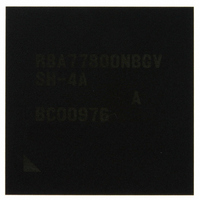
R8A77800ANBGAV Renesas Electronics America, R8A77800ANBGAV Datasheet - Page 661

R8A77800ANBGAV
Manufacturer Part Number
R8A77800ANBGAV
Description
IC SUPERH MPU ROMLESS 449-BGA
Manufacturer
Renesas Electronics America
Series
SuperH® SH7780r
Datasheet
1.R8A77800ANBGV.pdf
(1342 pages)
Specifications of R8A77800ANBGAV
Core Processor
SH-4A
Core Size
32-Bit
Speed
400MHz
Connectivity
Audio Codec, MMC, Serial Sound, SCI, SIO, SPI, SSI
Peripherals
DMA, POR, WDT
Number Of I /o
75
Program Memory Type
ROMless
Ram Size
16K x 8
Voltage - Supply (vcc/vdd)
1.15 V ~ 1.35 V
Oscillator Type
External
Operating Temperature
-20°C ~ 75°C
Package / Case
449-BGA
Lead Free Status / RoHS Status
Lead free / RoHS Compliant
Eeprom Size
-
Program Memory Size
-
Data Converters
-
Available stocks
Company
Part Number
Manufacturer
Quantity
Price
Company:
Part Number:
R8A77800ANBGAV
Manufacturer:
Renesas Electronics America
Quantity:
10 000
- Current page: 661 of 1342
- Download datasheet (7Mb)
14.5.4
The DACK output is divided to align the data unit like the CSn output when a DMA transfer unit
is divided with multiple bus cycles, for example when an 8-bit or 16-bit external device is
accessed in longword units, or when an 8-bit external device is accessed in word units, and the
CSn output is negated between these bus cycles.
14.5.5
To ensure that a DMINT interrupt source that should have been cleared is not inadvertently
accepted again, clear the BL bit after confirming the corresponding flag in INT2B3 register
becomes 0 or issue the RTE instruction.
14.5.6
When one DMA transfer is performed by multiple bus cycles*
to negate between bus cycles*
output is negated between bus cycles, the DREQ signal is not sampled correctly and malfunction
may occur.
Notes: 1. When a DMA transfer is performed with larger transfer size than the bus width. For
14.5.7
The DACK signal may be asserted ceaselessly during two or more times DMA transfer when the
DREQ level detection with overrun 1 and the DREQ edge detection. In this case, the DMA
transfer is suspended and do not perform correctly, to avoid this insert one or more idle cycle
between the DMA transfer.
The transfer source is the LBSC space and the DACK is output during the read cycle:
(1) Set B'001 to B'111 (i.e., other than 000) to the IWRRD bits in CSnBCR
(2) Set B'001 to B'111 (i.e., other than 000) to the IWRRS bits in CSnBCR
2. When the CSn output is negated between bus cycles, then the DACK output is also
DACK output division
Clear DMINT Interrupt
CS Output Settings and Transfer Size Larger than External Bus Width
DACK Assertion and DREQ Sampling
example, performing the 16-/32-byte transfer to the 8-/16-/32-bit bus width LBSC
space, longword (32-bit) transfer to the 8-/16-bit bus width LBSC space, or word (16-
bit) transfer to the 8-bit bus width LBSC space. Note that except for a 32-bit access to
the MPX interface. This access generates only one bus cycle (burst).
negated between bus cycles (DACK output is also divided).
2
. For detail of settings, refer to table 11.11 to 11.14. If set the CSn
Section 14 Direct Memory Access Controller (DMAC)
Rev.1.00 Dec. 13, 2005 Page 609 of 1286
1
, the CSn output should be set not
REJ09B0158-0100
Related parts for R8A77800ANBGAV
Image
Part Number
Description
Manufacturer
Datasheet
Request
R

Part Number:
Description:
KIT STARTER FOR M16C/29
Manufacturer:
Renesas Electronics America
Datasheet:

Part Number:
Description:
KIT STARTER FOR R8C/2D
Manufacturer:
Renesas Electronics America
Datasheet:

Part Number:
Description:
R0K33062P STARTER KIT
Manufacturer:
Renesas Electronics America
Datasheet:

Part Number:
Description:
KIT STARTER FOR R8C/23 E8A
Manufacturer:
Renesas Electronics America
Datasheet:

Part Number:
Description:
KIT STARTER FOR R8C/25
Manufacturer:
Renesas Electronics America
Datasheet:

Part Number:
Description:
KIT STARTER H8S2456 SHARPE DSPLY
Manufacturer:
Renesas Electronics America
Datasheet:

Part Number:
Description:
KIT STARTER FOR R8C38C
Manufacturer:
Renesas Electronics America
Datasheet:

Part Number:
Description:
KIT STARTER FOR R8C35C
Manufacturer:
Renesas Electronics America
Datasheet:

Part Number:
Description:
KIT STARTER FOR R8CL3AC+LCD APPS
Manufacturer:
Renesas Electronics America
Datasheet:

Part Number:
Description:
KIT STARTER FOR RX610
Manufacturer:
Renesas Electronics America
Datasheet:

Part Number:
Description:
KIT STARTER FOR R32C/118
Manufacturer:
Renesas Electronics America
Datasheet:

Part Number:
Description:
KIT DEV RSK-R8C/26-29
Manufacturer:
Renesas Electronics America
Datasheet:

Part Number:
Description:
KIT STARTER FOR SH7124
Manufacturer:
Renesas Electronics America
Datasheet:

Part Number:
Description:
KIT STARTER FOR H8SX/1622
Manufacturer:
Renesas Electronics America
Datasheet:

Part Number:
Description:
KIT DEV FOR SH7203
Manufacturer:
Renesas Electronics America
Datasheet:


