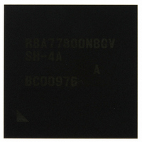
R8A77800ANBGAV Renesas Electronics America, R8A77800ANBGAV Datasheet - Page 385

R8A77800ANBGAV
Manufacturer Part Number
R8A77800ANBGAV
Description
IC SUPERH MPU ROMLESS 449-BGA
Manufacturer
Renesas Electronics America
Series
SuperH® SH7780r
Datasheet
1.R8A77800ANBGV.pdf
(1342 pages)
Specifications of R8A77800ANBGAV
Core Processor
SH-4A
Core Size
32-Bit
Speed
400MHz
Connectivity
Audio Codec, MMC, Serial Sound, SCI, SIO, SPI, SSI
Peripherals
DMA, POR, WDT
Number Of I /o
75
Program Memory Type
ROMless
Ram Size
16K x 8
Voltage - Supply (vcc/vdd)
1.15 V ~ 1.35 V
Oscillator Type
External
Operating Temperature
-20°C ~ 75°C
Package / Case
449-BGA
Lead Free Status / RoHS Status
Lead free / RoHS Compliant
Eeprom Size
-
Program Memory Size
-
Data Converters
-
Available stocks
Company
Part Number
Manufacturer
Quantity
Price
Company:
Part Number:
R8A77800ANBGAV
Manufacturer:
Renesas Electronics America
Quantity:
10 000
- Current page: 385 of 1342
- Download datasheet (7Mb)
The instruction to modify the value of the MMSELR should be allocated non-cacheable P2 area
and an address that will not be affected by an address map change.
Write to MMSELR before enabling the Instruction cache, Operand cache, and MMU address
translation, and then do not write to it again until after power-on reset or manual reset.
11.4.2
BCR is a 32-bit readable/writable register that specifies the function and bus cycle status for each
area. BCR is initialized to H'0000 0000 in big endian or H'8000 0000 in little endian by a power-
on reset, but is not initialized by a manual reset mode.
Initial value:
Initial value:
Bit
31
30 to 27
Note: * The intial value of the endian bit (bit 31) depends on the MODE5 pin setting.
R/W:
R/W:
Bit:
Bit:
Bus Control Register (BCR)
Bit Name
ENDIAN
R/W
END
0/1*
IAN
31
15
—
R
0
R/W
CNT
HIZ
30
14
—
R
0
0
Initial
Value
0/1
All 0
29
13
—
—
R
R
0
0
28
12
—
—
R
R
0
0
27
11
—
—
R
R
0
0
R/W
R
R
DPUP
R/W
26
10
—
R
0
0
Description
Endian Flag
The value of the external pin (MODE5) designating the
endian mode is sampled at a power-on reset by the
PRESET pin. This bit determines the endian mode of all
spaces.
0: Indicates that the external pin (MODE5) designating
1: Indicates that the external pin (MODE5) designating
Reserved
These bits are always read as 0. The write value should
always be 0.
25
—
—
R
R
0
9
0
the endian mode is low at a power-on reset and big-
endian mode is specified for this LSI.
the endian mode is high at a power-on reset and
little-endian mode is specified for this LSI.
OPUP
R/W
24
—
R
0
8
0
R/W
23
—
R
0
7
0
Section 11 Local Bus State Controller (LBSC)
DACKBST[3:0]
Rev.1.00 Dec. 13, 2005 Page 333 of 1286
R/W
R/W
22
0
6
0
R/W
R/W
21
0
5
0
R/W
R/W
20
0
4
0
ASYNC[6:0]
R/W
19
—
R
0
3
0
REJ09B0158-0100
R/W
18
—
R
0
2
0
BREQ
R/W
R/W
EN
17
0
1
0
R/W
R/W
DMA
BST
16
0
0
0
Related parts for R8A77800ANBGAV
Image
Part Number
Description
Manufacturer
Datasheet
Request
R

Part Number:
Description:
KIT STARTER FOR M16C/29
Manufacturer:
Renesas Electronics America
Datasheet:

Part Number:
Description:
KIT STARTER FOR R8C/2D
Manufacturer:
Renesas Electronics America
Datasheet:

Part Number:
Description:
R0K33062P STARTER KIT
Manufacturer:
Renesas Electronics America
Datasheet:

Part Number:
Description:
KIT STARTER FOR R8C/23 E8A
Manufacturer:
Renesas Electronics America
Datasheet:

Part Number:
Description:
KIT STARTER FOR R8C/25
Manufacturer:
Renesas Electronics America
Datasheet:

Part Number:
Description:
KIT STARTER H8S2456 SHARPE DSPLY
Manufacturer:
Renesas Electronics America
Datasheet:

Part Number:
Description:
KIT STARTER FOR R8C38C
Manufacturer:
Renesas Electronics America
Datasheet:

Part Number:
Description:
KIT STARTER FOR R8C35C
Manufacturer:
Renesas Electronics America
Datasheet:

Part Number:
Description:
KIT STARTER FOR R8CL3AC+LCD APPS
Manufacturer:
Renesas Electronics America
Datasheet:

Part Number:
Description:
KIT STARTER FOR RX610
Manufacturer:
Renesas Electronics America
Datasheet:

Part Number:
Description:
KIT STARTER FOR R32C/118
Manufacturer:
Renesas Electronics America
Datasheet:

Part Number:
Description:
KIT DEV RSK-R8C/26-29
Manufacturer:
Renesas Electronics America
Datasheet:

Part Number:
Description:
KIT STARTER FOR SH7124
Manufacturer:
Renesas Electronics America
Datasheet:

Part Number:
Description:
KIT STARTER FOR H8SX/1622
Manufacturer:
Renesas Electronics America
Datasheet:

Part Number:
Description:
KIT DEV FOR SH7203
Manufacturer:
Renesas Electronics America
Datasheet:


