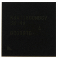
R8A77800ANBGAV Renesas Electronics America, R8A77800ANBGAV Datasheet - Page 243

R8A77800ANBGAV
Manufacturer Part Number
R8A77800ANBGAV
Description
IC SUPERH MPU ROMLESS 449-BGA
Manufacturer
Renesas Electronics America
Series
SuperH® SH7780r
Datasheet
1.R8A77800ANBGV.pdf
(1342 pages)
Specifications of R8A77800ANBGAV
Core Processor
SH-4A
Core Size
32-Bit
Speed
400MHz
Connectivity
Audio Codec, MMC, Serial Sound, SCI, SIO, SPI, SSI
Peripherals
DMA, POR, WDT
Number Of I /o
75
Program Memory Type
ROMless
Ram Size
16K x 8
Voltage - Supply (vcc/vdd)
1.15 V ~ 1.35 V
Oscillator Type
External
Operating Temperature
-20°C ~ 75°C
Package / Case
449-BGA
Lead Free Status / RoHS Status
Lead free / RoHS Compliant
Eeprom Size
-
Program Memory Size
-
Data Converters
-
Available stocks
Company
Part Number
Manufacturer
Quantity
Price
Company:
Part Number:
R8A77800ANBGAV
Manufacturer:
Renesas Electronics America
Quantity:
10 000
- Current page: 243 of 1342
- Download datasheet (7Mb)
• C: Cacheability bit
• WT: Write-through bit
• UB: Buffered write bit
7.7.4
This LSI supports the following PMB functions.
1. Only memory-mapped write can be used for writing to the PMB. The LDTLB instruction
2. Software must ensure that every accessed P1 or P2 address has a corresponding PMB entry
3. This LSI does not guarantee the operation when multiple hit occurs in the PMB. Special care
4. The PMB does not have an associative write function.
5. Since there is no PR field in the PMB, read/write protection cannot be preformed. The address
6. Both entries from the UTLB and PMB are mixed and recorded in the ITLB by means of the
With a 512-Mbyte page, PPN[31:29] are valid.
Indicates whether a page is cacheable.
0: Not cacheable
1: Cacheable
Specifies the cache write mode.
0: Copy-back mode
1: Write-through mode
Specifies whether a buffered write is performed.
0: Buffered write (Data access of subsequent processing proceeds without waiting for the write
1: Unbuffered write (Data access of subsequent processing is stalled until the write has
cannot be used to write to the PMB.
before the access occurs. When an access to an address in the P1 or P2 area which is not
recorded in the PMB is made, this LSI is reset by the TLB. In this case, the accessed address in
the P1 or P2 area which causes the TLB reset is stored in the TEA and code H′140 in the
EXPEVT.
should be taken when the PMB mapping information is recorded by software.
translation target of the PMB is the P1 or P2 address. In user mode access, an address error
exception occurs.
hardware ITLB miss handling. However, these entries can be identified by checking whether
to complete.)
completed.)
PMB Function
Section 7 Memory Management Unit (MMU)
Rev.1.00 Dec. 13, 2005 Page 191 of 1286
REJ09B0158-0100
Related parts for R8A77800ANBGAV
Image
Part Number
Description
Manufacturer
Datasheet
Request
R

Part Number:
Description:
KIT STARTER FOR M16C/29
Manufacturer:
Renesas Electronics America
Datasheet:

Part Number:
Description:
KIT STARTER FOR R8C/2D
Manufacturer:
Renesas Electronics America
Datasheet:

Part Number:
Description:
R0K33062P STARTER KIT
Manufacturer:
Renesas Electronics America
Datasheet:

Part Number:
Description:
KIT STARTER FOR R8C/23 E8A
Manufacturer:
Renesas Electronics America
Datasheet:

Part Number:
Description:
KIT STARTER FOR R8C/25
Manufacturer:
Renesas Electronics America
Datasheet:

Part Number:
Description:
KIT STARTER H8S2456 SHARPE DSPLY
Manufacturer:
Renesas Electronics America
Datasheet:

Part Number:
Description:
KIT STARTER FOR R8C38C
Manufacturer:
Renesas Electronics America
Datasheet:

Part Number:
Description:
KIT STARTER FOR R8C35C
Manufacturer:
Renesas Electronics America
Datasheet:

Part Number:
Description:
KIT STARTER FOR R8CL3AC+LCD APPS
Manufacturer:
Renesas Electronics America
Datasheet:

Part Number:
Description:
KIT STARTER FOR RX610
Manufacturer:
Renesas Electronics America
Datasheet:

Part Number:
Description:
KIT STARTER FOR R32C/118
Manufacturer:
Renesas Electronics America
Datasheet:

Part Number:
Description:
KIT DEV RSK-R8C/26-29
Manufacturer:
Renesas Electronics America
Datasheet:

Part Number:
Description:
KIT STARTER FOR SH7124
Manufacturer:
Renesas Electronics America
Datasheet:

Part Number:
Description:
KIT STARTER FOR H8SX/1622
Manufacturer:
Renesas Electronics America
Datasheet:

Part Number:
Description:
KIT DEV FOR SH7203
Manufacturer:
Renesas Electronics America
Datasheet:


